Download
1 / 26
270 likes | 518 Views
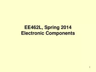
EE462L, Spring 2014 DC−DC SEPIC (Converter). !. + v C1 –. + v L1 –. i. I. in. out. C. +. + v L2 –. L1. C1. V. V. out. in. C. L2. –. + v C1 –. + v L2 –. C1. L2. Boost converter. + v L1 –. i. I. out. in. +. L1. V. V. out. in. –. SEPIC converter. !.

E N D
! + v C1– + v L1– i I in out C + + v L2 – L1 C1 V V out in C L2 – + v C1– + v L2 – C1 L2 Boost converter + v L1– i I out in + L1 V V out in – SEPIC converter
! + v C1– + v L1– i I in out + + v L2 – L1 C1 V V out in C L2 – SEPIC converter SEPIC = single ended primary inductor converter This circuit is more unforgiving than the boost converter, because the MOSFET and diode voltages and currents are higher • Before applying power, make sure that your D is at the minimum, and that a load is solidly connected • Limit your output voltage to 90V
KVL and KCL in the average sense + Vin– + 0– I I I in 0 out out + L1 + 0 – C1 I out V V out in I C 0 L2 in – KVL shows that VC1 = Vin Interestingly, no average current passes from the source side, through C1, to the load side, and yet this is a “DC - DC” converter
I out + V out C – Switch closed assume constant + Vin– + Vin– + v D– i in + v L2 – L1 C1 V in L2 KVL shows that vD = −(Vin + Vout), so the diode is open Thus, C is providing the load power when the switch is closed + Vin– – (Vin + Vout) + + Vin– i I in out + – Vin + L1 C1 V V out in C I L2 out – iL1 and iL2 are ramping up (charging). C1 is charging L2 (so C1 is discharging). C is also discharging.
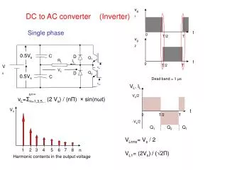
! Switch open (assume the diode is conducting because, otherwise, the circuit cannot work) assume constant + Vin– – Vout+ i I out in + + L1 C1 V V V out out in C L2 – – C1 and C are charging. L1 and L2 are discharging. KVL shows that VL1 = −Vout The input/output equation comes from recognizing that the average voltage across L1 is zero Voltage can be stepped-up or stepped-down
i i in d + ! – V V i i L C in out C L – + I out The buck-boost converter Inverse polarity with respect to input • Compared with SEPIC: • + Fewer energy storage components • + Capacitor does not carry load current • + In both converters isolation can be easily implemented • - Polarity is reversed Voltage can be stepped-up or stepped-down
Inductor L1 current rating During the “on” state, L1 operates under the same conditions as the boost converter L, so the results are the same Use max
Inductor L2 current rating Average values + Vin– + 0– I I I in 0 out out + L1 + 0 – C1 I out V V out in I C 0 L2 in – iL2 2Iout Iavg = Iout ΔI 0 Use max
+ v C1– + v L2 – C1 L2 MOSFET and diode currents and current ratings + v L1– i I in out + L1 V V out in C – iL1 + iL2 MOSFET Diode iL1 + iL2 2(Iin + Iout) 2(Iin + Iout) 0 0 switch closed switch open Take worst case D for each Use max
Output capacitor C current and current rating iC = (iD – Iout) 2Iin + Iout 0 −Iout switch closed switch open As D → 0, Iin<< Iout , so As D → 1, Iin>> Iout , so
Series capacitor C1 current and current rating + Vin– – (Vin + Vout) + + Vin– i I in out + – Vin + L1 C1 V V out in C I L2 out – + Vin– – Vout+ i I out in + + L1 C1 V V V out out in C L2 – – Switch closed, IC1 = −IL2 Switch open, IC1 = IL1
! Series capacitor C1 current and current rating Switch closed, IC1 = −IL2 iC1 Switch open, IC1 = IL1 2Iin switch closed 0 switch open −2Iout As D → 1, Iin>> Iout , so As D → 0, Iin<< Iout , so The high capacitor current rating is a disadvantage of this converter
Worst-case load ripple voltage iC = (iD – Iout) 0 −Iout The worst case is where D → 1, where output capacitor C provides Iout for most of the period. Then,
Worst case ripple voltage on series capacitor C1 iC1 switch open 2Iin 0 −2Iout switch closed Then, considering the worst case (i.e., D = 1)
Voltage ratings + Vin– – (Vin + Vout) + + L1 C1 V V out in C L2 – MOSFET and diode see (Vin + Vout) + Vin– – Vout+ + L1 C1 V V out in C L2 – • Diode and MOSFET, use 2(Vin + Vout) • Capacitor C1, use 1.5Vin • Capacitor C, use 1.5Vout
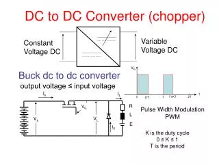
Continuous current in L1 iL 2Iin Iavg = Iin 0 (1 − D)T Then, considering the worst case (i.e., D → 1), use max guarantees continuous conduction use min
Continuous current in L2 iL 2Iout Iavg = Iout 0 (1 − D)T Then, considering the worst case (i.e., D → 0), use max guarantees continuous conduction use min
Impedance matching Iin DC−DC Boost Converter + − + Vin − Source Iin + Vin − Equivalent from source perspective
! Impedance matching For any Rload, as D → 0, then Requiv → ∞ (i.e., an open circuit) For any Rload, as D → 1, then Requiv → 0 (i.e., a short circuit) Thus, the SEPIC converter can sweep the entire I-V curve of a solar panel
Example - connect a 100Ω load resistor D = 0.88 D = 0.80 2Ω equiv. 6.44Ω equiv. D = 0.50 100Ω equiv. With a 100Ω load resistor attached, raising D from 0 to 1 moves the solar panel load from the open circuit condition to the short circuit condition
Example - connect a 5Ω load resistor D = 0.61 D = 0.47 2Ω equiv. 6.44Ω equiv. D = 0.18 100Ω equiv.
Our components 9A 250V 5.66A p-p 200V, 250V 16A, 20A 10A 90V 10A, 5A 40V, 90V 10A, 5A Likely worst-case SEPIC situation L2. 100µH, 9A L1. 100µH, 9A C1. 33µF, 50V, 14A p-p C. 1500µF, 250V, 5.66A p-p Diode D. 200V, 16A MOSFET M. 250V, 20A SEPIC DESIGN
SEPIC DESIGN 5A 0.067V 1500µF 50kHz L2. 100µH, 9A L1. 100µH, 9A C1. 33µF, 50V, 14A p-p C. 1500µF, 250V, 5.66A p-p Diode D. 200V, 16A MOSFET M. 250V, 20A
SEPIC DESIGN 40V 90V 200µH 450µH 2A 50kHz 2A 50kHz L2. 100µH, 9A L1. 100µH, 9A C1. 33µF, 50V, 14A p-p C. 1500µF, 250V, 5.66A p-p Diode D. 200V, 16A MOSFET M. 250V, 20A
50V 14A p-p Our components 9A 5A 3.0V 40V 33µF 10A 5A 5A 50kHz Likely worst-case SEPIC situation SEPIC DESIGN SEPIC converter L2. 100µH, 9A L1. 100µH, 9A C1. 33µF, 50V, 14A p-p C. 1500µF, 250V, 5.66A p-p Diode D. 200V, 16A Conclusion - 50kHz may be too low for SEPIC converter MOSFET M. 250V, 20A