Download
1 / 18
470 likes | 1.35k Views
Thin film solar cells. Presented by Yao Sun. Future energy source. Clean energy Most reasonable price for the future Available anywhere in the world 1.52*10^21 KWh. Drivers for Thin-film Solar Cells. Ever-rising price for fossil fuels and global warming

E N D
Thin film solar cells Presented by Yao Sun
Future energy source • Clean energy • Most reasonable price for the future • Available anywhere in the world • 1.52*10^21 KWh
Drivers for Thin-film Solar Cells • Ever-rising price for fossil fuels and global warming • Shortage of silicon feedstock for wafer-based solar cells -Will continue until 2010 • Public awareness of clean energy -and green manufacturing technology -Thin-film cells cost less energy to make • Much lower materials consumption with thin-film cells -Manufacturing cost is a big issue with wafer-based
Thin Film Solar Cell • Use less than 10% of raw material compared to wafer based solar cell. • Using glass as substrate which reduce the initial cost. • Possible to deposit the cells on all kind of materials, which opens a new dimension for new application. • Size is not a limit factor • Possible to deposit the cell onto curvature substrate (glass), this advantage make a lot applications possible. Example Cell onto the vehicle glass. Cell onto the building glass.
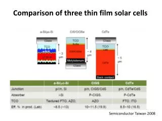
Mature Thin-film PV Technologies • Amorphous Si solar cell • Polycrystalline Si solar cell • Cadmium telluride(CdTe) • Copper-indium selenide(CIS) • Cu ( In1-xGax ) Se2
Band gap • 1. Conduction band • 2. Valence band
Direct band gap& Indirect band gap Conduction band Energy Valence band Momentum An electron can shift from the lowest-energy state in the conduction band (green) to the highest-energy state in the valence band (red) without a change in momentum.
Indirect band gap Energy Conduction Band Valence Band Momentum Hard to happen Low efficiency
Light trapping Low power conversion efficiency -thin film thickness -indirect band gap Light trapping -is defined as path length enhancement in the bulk regions of the cell -equivalent to increasing the thickness -minority carriers need to diffuse over a shorter distance to reach the electrodes
Light trapping schemes • http://pvcdrom.pveducation.org/DESIGN/LITETRAP.HTM Backside mirrors Randomizing surfaces Textured surfaces Using total internal reflection, light can be trapped inside the cell and make multiple passes through the cell, thus allowing even a thin solar cell to maintain a high optical path length.
Randomizing surface Textured surface • -creating oblique surface with opposite slopes • -forming grooves at the top surface • -perfectly randomizing surfaces are difficult to realize • -simplest way is to tilt one surface relative to the other • -lower degree of symmetry renders greater degree of light trapping
Practical schemes • Reflective back surfaces -metalizing the back surface of the cell with Al or Au. -can be improved by inserting an oxide layer between semiconductor and metal Front surface texturing -wet etching Texturing back surface -growing the active layer on patterned substrates or gratings
Two important light trapping schemes in commercial solar cells Laser fired contact Crystalline Si on glass (CSG) • Thermal oxide layer inserted between the Si device layer and Al metal layer • Passivates the back surface • Enhances Al reflection • Using polycrystalline Si crystallized from amorphous Si as the active layer • Textured glass substrate and a rear reflector
I thought you may interested in this. Cell/Module Makers Wafer-based A-Si thin-film CdTe thin-film http://www.miasole.com/www/index.shtml# CIGS thin-film CIGS nano-particle