Download
1 / 23
230 likes | 1.02k Views
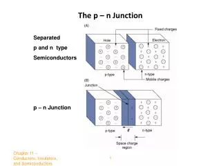
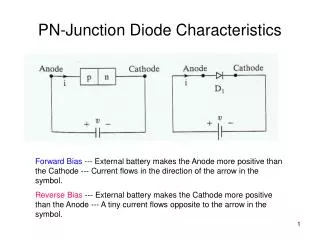
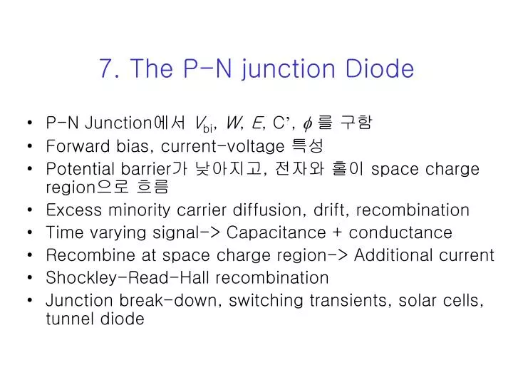
7. The P-N junction Diode P-N Junction 에서 V bi , W , E , C ’ , f 를 구함 Forward bias, current-voltage 특성 Potential barrier 가 낮아지고 , 전자와 홀이 space charge region 으로 흐름 Excess minority carrier diffusion, drift, recombination Time varying signal-> Capacitance + conductance

E N D
7. The P-N junction Diode • P-N Junction에서 Vbi, W, E, C’, f를 구함 • Forward bias, current-voltage 특성 • Potential barrier가 낮아지고, 전자와 홀이 space charge region으로 흐름 • Excess minority carrier diffusion, drift, recombination • Time varying signal-> Capacitance + conductance • Recombine at space charge region-> Additional current • Shockley-Read-Hall recombination • Junction break-down, switching transients, solar cells, tunnel diode
7.1 Ideal Current-Voltage Relationship • Abrupt depletion layer 근사, space charge region 외에는 neutral • Maxwell-Boltzmann 근사 • Low injection 가정 • Current: • Total current is a constant • 전자와 홀의 전류는 연속 함수 • 이번 장에서의 기본적인 가정
7.1.1 경계 조건 완전 이온화라면 N 부분에서의 열적 평형 상태의 Majority 운반자 전자의 농도 P 부분에서 minority 운반자 전자의 농도는 P 부분에서의 minority 운반자 전자의 농도와 N 부분에서의 majority 운반자인 전자 농도의 관계 (열적 평형 상태)
Positive Voltage -> potential barrier 가 낮아짐 (그림 7.2) • Eapp가 space charge region의 전기장과 반대 방향 • 알짜 전기장 감소 • Diffusion과 전기장에 의한 힘의 균형이 무너짐 • N 쪽에 있던 전자들이 p 쪽으로 inject 되기 시작 (홀에 대해서도 마찬가지) • P 부분에서의 minority 운반자 전자의 농도 • (Space charge region의 edge 에서, 열적 평형 상태가 아님) • 인가한 전기장에 따라서 지수 함수적으로 증가
이때 p 부분의 초과 전자들은 확산과 재결합 과정을 겪게 된다. • N 부분에서의 초과 홀의 농도는 유사한 식으로 정해짐 • 위의 결과는 reverse bias에 대해서도 성립
7.1.2 Minority Carrier의 분포 • Ch. 5에서 배운 내용을 이용 (n 부분에서 초과 운반자인 홀에 대해서, ambipolar transport 방정식 • Ch. 4 Drift current density, in the n 범위, E=0, g’=0, steady state
이때 경계 조건들 최종 결과
7.1.2 Ideal PN junction 전류 • 전체 전류는 전자와 홀의 합 • 전자와 홀의 전류는 depletion region 에서 상수 • 전체 전류는 minority 홀 diffusion current at x=xn+ minority 전자 at x = -xp • Depletion region 외부에서는 전기장을 0으로 가정, 따라서 확산에 의한 diffusion 전류가 중요
마찬가지로 x=-xp에서 전자에 대해 풀면 이때 전자와 홀에 대한 전류 모두 +x 방향 Ideal current-voltage 관계식, 전체 전류: 전자 + 홀 Js: Reverse Saturation Current Density 그림 7.6
7.1.4 Physics 요약 • Forward bias: • potential barrier을 낮춤 • 전자와 홀이 space charge region으로 injected 됨 • Inject 된 전자와 홀은 minority 운반자가 되고, 확산을 통해서 majority 운반자와 재결합. Current density p n Jtotal Majority 홀 전류 Majority 전자 전류 Jn(-xp) Jp(xn) 전자의 Diffusion 전류 홀의 Diffusion 전류 x=0 xn -xp
예제 7.4 주어진 majority 운반자의 drift current을 생성하기 위한 전기장의 크기를 구하는 문제 • 앞의 유도 과정에서 pn 정션의 space charge region외의 neutral 부분은 전기장이 0 이라고 가정. • 실제로는0은 아니지만, 굉장히 작은값이므로 좋은 근사임을 이 문제를 통하여서 확인
7.1.5 Temperature effects • Ideal reverse saturation current density • Function of ni2 • Strongly depends on Temp. • For forward bias, exp(eVa/kBT) term • Less sensitive
n p Wn 7.1.6 The “Short” Diode • 앞에서 p, n 부분이 diffusion length보다 훨씬 길다고 가정 • 많은 경우 한 부분이 짧을 수 있음 • 새로운 경계 조건 at x=xn + Wn • Ohmic contact at (x=xn + Wn): Infinite surface recombination velocity-> no 초과 minority carrier
일반해는 마찬가지로 지수 함수 꼴이지만, 경계 조건이 달라지면서 해의 형태가 조금 바뀜 • For Wn>> Ln : 원래 식으로 환원 • For Wn<< Ln : sinh(x)~x 이용, 선형관계 얻음 • 이 경우에 Diffusion current을 구해보면 • 이 식의 물리적 의미 • Larger diffusion current for short diode • Diffusion current : 상수 • No recombination of minority 운반자
7.2 Small signal model 7.2.1 Diffusion Resistance • 여태까지 DC 만 고려, But 실질적인 경우 AC 성분 필요 ID:Diode current IS:Diode reverse saturation current • Assume applied dc V0 producing a dc IDQ • If superimpose small, low-frequency sinusoidal voltage • Small sinusoidal current will be added to dc. • Incremental conductance : sinusoidal current/sinusoidal voltage • For small signal Incremental conductance Incremental resistance
With sufficient bias voltage, we can neglect –1 term IDQ는 DC quiescent diode current • Incremental resistance : • Bias 의 함수 • Diffusion resistance라고도 함 • I-V curve의 기울기의 역수 (그림 7.10)
7.2.2 Small-Signal Admittance (Impedance) • Forward bias에 대한 Impedance를 minority 운반자의 diffusion current를 이용해서 계산 • minority 운반자의 diffusion current를 additional small ac signal에 대해서 계산 • Set x=0 at the xn (계산상의 편의를 위해서)
지수 함수 term을 Talyor 전개 Time dependent diffusion 방정식의 경계 조건을 사용 N-region (x>0), E=0, Diffusion 방정식: 인가 ac 전압이 사인 함수, steady state 해 역시 사인 함수 형태 p1(x) : 초과 운반자 농도의 ac 성분의 크기
첫번째 항: dc 에 대한 해를 만족 경계 조건 p1(x->infinity)=0, and p1(x=0) 식 (7.41)
이제 홀 diffusion current density를 구해보자 식 (7.18)
전체 홀 전류의 크기 전자에 대해서 p-region 에서 구하면 전체 전류: 홀과 전자에 의한 전류의 합
전체 Admittance (Impedance): 여기서 진동수가 충분히 작다면 Diffusion conductance: Diffusion Capacitance:
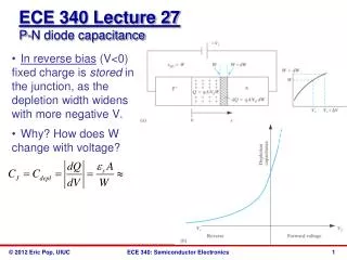
7.2.3 Equivalent Circuit • pn 정션을 등가 회로로 대치 • 회로 분석시 유용 rs rd Cd rd : Diffusion resistance Cd : Diffusion capacitance Cj : Junction capacitance rs : finite resistance at depletion region 외부 Cj Va Vapp