Download
1 / 29
300 likes | 329 Views
The Junction Diode. BY Prof. Vhangade B.U. M.P.A.S.C.College,panvel.

E N D
The Junction Diode BY Prof. Vhangade B.U.M.P.A.S.C.College,panvel
In electronics, a diode is a component that restricts the direction of movement of charge carriers. Essentially, it allows an electric current to flow in one direction, but blocks it in the opposite direction. Thus, the diode can be thought of as an electronic version of a check valve. Circuits that require current flow in only one direction will typically include one or more diodes in the circuit design.
Short history • Thermionic and solid state diodes developed in parallel. The principle of operation of thermionic diodes was discovered by Frederick Guthrie in 1873. The principle of operation of crystal diodes was discovered in 1874 by the German scientist, Karl Ferdinand Braun. • Thermionic diode principles were rediscovered by Thomas Edison on February 13, 1880 and he took out a patent in 1883, but developed the idea no further. Braun patented the crystal rectifier in 1899. The first radio receiver using a crystal diode was built around 1900 by Greenleaf Whittier Pickard. The first thermionic diode was patented in Britain by John Ambrose Fleming (scientific adviser to the Marconi Company and former Edison employee on November 16, 1904. Pickard received a patent for a silicon crystal detector on November 20, 1906. • At the time of their invention such devices were known as rectifiers. In 1919William Henry Eccles coined the term diode from Greek roots; di means 'two', and ode (from odos) means 'path'.
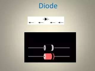
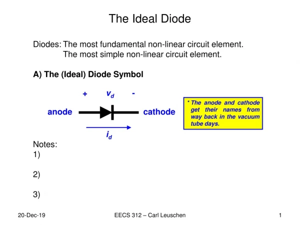
Diode schematic symbol Current can flow from the anode to the cathode, but not the other way around. Most modern diodes are based on semiconductorp-n junctions. In a p-n diode, conventional current can flow from the p-type side (the anode) to the n-type side (the cathode), but not in the opposite direction. Another type of semiconductor diode, the Schottky diode, is formed from the contact between a metal and a semiconductor rather than by a p-n junction.
A semiconductor diode's current-voltage, or I-V, characteristic curve is ascribed to the behavior of the so-called depletion layer or depletion zone which exists at the p-n junction between the differing semiconductors. When a p-n junction is first created, conduction band (mobile) electrons from the N-doped region diffuse into the P-doped region where there is a large population of holes (places for electrons in which no electron is present) with which the electrons "recombine". When a mobile electron recombines with a hole, the hole vanishes and the electron is no longer mobile. Thus, two charge carriers have vanished. The region around the p-n junction becomes depleted of charge carriers and thus behaves as an insulator.
However, the depletion width cannot grow without limit. For each electron-hole pair that recombines, a positively-charged dopant ion is left behind in the N-doped region, and a negatively charged dopant ion is left behind in the P-doped region. As recombination proceeds and more ions are created, an increasing electric field develops through the depletion zone which acts to slow and then finally stop recombination. At this point, there is a 'built-in' potential across the depletion zone.
If an external voltage is placed across the diode with the same polarity as the built-in potential, the depletion zone continues to act as an insulator preventing a significant electric current. This is the reverse bias phenomenon. However, if the polarity of the external voltage opposes the built-in potential, recombination can once again proceed resulting in substantial electric current through the p-n junction. For silicon diodes, the built-in potential is approximately 0.6 V. Thus, if an external current is passed through the diode, about 0.6 V will be developed across the diode such that the P-doped region is positive with respect to the N-doped region and the diode is said to be 'turned on' as it has a forward bias.
A diode's I-V characteristic can be approximated by two regions of operation. Below a certain difference in potential between the two leads, the depletion layer has significant width, and the diode can be thought of as an open (non-conductive) circuit. As the potential difference is increased, at some stage the diode will become conductive and allow charges to flow, at which point it can be thought of as a connection with zero (or at least very low) resistance. More precisely, the transfer function is logarithmic, but so sharp that it looks like a corner on a zoomed-out graph.
In a normal silicon diode at rated currents, the voltage drop across a conducting diode is approximately 0.6 to 0.7 volts. The value is different for other diode types - Schottky diodes can be as low as 0.2 V and light-emitting diodes (LEDs) can be 1.4 V or more (Blue LEDs can be up to 4.0 V). Referring to the I-V characteristics image, in the reverse bias region for a normal P-N rectifier diode, the current through the device is very low (in the µA range) for all reverse voltages up to a point called the peak-inverse-voltage (PIV). Beyond this point a process called reverse breakdown occurs which causes the device to be damaged along with a large increase in current. For special purpose diodes like the avalanche or zener diodes, the concept of PIV is not applicable since they have a deliberate breakdown beyond a known reverse current such that the reverse voltage is "clamped" to a known value (called the zener voltage or breakdown voltage). These devices however have a maximum limit to the current and power in the zener or avalanche region.
Some types of semiconductor diode • Normal (p-n) diodes • which operate as described above. Usually made of doped silicon or, more rarely, germanium. Before the development of modern silicon power rectifier diodes, cuprous oxide and later selenium was used; its low efficiency gave it a much higher forward voltage drop (typically 1.4–1.7 V per "cell," with multiple cells stacked to increase the peak inverse voltage rating in high voltage rectifiers), and required a large heat sink (often an extension of the diode's metal substrate), much larger than a silicon diode of the same current ratings would require.
Schottky diodes • Schottky diodes are constructed from a metal to semiconductor contact. They have a lower forward voltage drop than a standard PN junction diode. Their forward voltage drop at forward currents of about 1 mA is in the range 0.15 V to 0.45 V, which makes them useful in voltage clamping applications and prevention of transistor saturation. They can also be used as low loss rectifiers although their reverse leakage current is generally much higher than non Schottky rectifiers. They also tend to have much lower junction capacitance than PN diodes and this contributes towards their high switching speed and their suitability in high speed circuits and RF devices such as mixers and detectors.
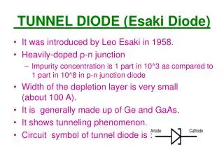
Esaki or tunnel diodes • These have a region of operation showing negative resistance caused by quantum tunneling, thus allowing amplification of signals and very simple bistable circuits. These diodes are also the type most resistant to nuclear radiation. • Gunn diodes • These are similar to tunnel diodes in that they are made of materials such as GaAs or InP that exhibit a region of negative differential resistance. With appropriate biasing, dipole domains form and travel across the diode, allowing high frequency microwaveoscillators to be built.
Light-emitting diodes (LEDs) • In a diode formed from a direct band-gap semiconductor, such as gallium arsenide, carriers that cross the junction emit photons when they recombine with the majority carrier on the other side. Depending on the material, wavelengths (or colors) from the infrared to the near ultraviolet may be produced. The forward potential of these diodes depends on the wavelength of the emitted photons: 1.2 V corresponds to red, 2.4 to violet. The first LEDs were red and yellow, and higher-frequency diodes have been developed over time. All LEDs are monochromatic; 'white' LEDs are actually combinations of three LEDs of a different color, or a blue LED with a yellow scintillator coating. LEDs can also be used as low-efficiency photodiodes in signal applications. An LED may be paired with a photodiode or phototransistor in the same package, to form an opto-isolator
Laser diodes • When an LED-like structure is contained in a resonant cavity formed by polishing the parallel end faces, a laser can be formed. Laser diodes are commonly used in optical storage devices and for high speed optical communication.
Photodiodes • Semiconductors are subject to optical charge carrier generation and therefore most are packaged in light blocking material. If they are packaged in materials that allow light to pass, their photosensitivity can be utilized. Photodiodes can be used as solar cells, and in photometry.
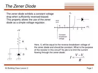
Zener diodes • Diodes that can be made to conduct backwards. This effect, called Zener breakdown, occurs at a precisely defined voltage, allowing the diode to be used as a precision voltage reference. In practical voltage reference circuits Zener and switching diodes are connected in series and opposite directions to balance the temperature coefficient to near zero. Some devices labeled as high-voltage Zener diodes are actually avalanche diodes. Two (equivalent) Zeners in series and in reverse order, in the same package, constitute a transient absorber (or Transorb, a registered trademark). They are named for Dr. Clarence Melvin Zener of Southern Illinois University, inventor of the device.
Varicap or varactor diodes • These are used as voltage-controlled capacitors. These are important in PLL (phase-locked loop) and FLL (frequency-locked loop) circuits, allowing tuning circuits, such as those in television receivers, to lock quickly, replacing older designs that took a long time to warm up and lock. A PLL is faster than a FLL, but prone to integer harmonic locking (if one attempts to lock to a broadband signal). They also enabled tunable oscillators in early discrete tuning of radios, where a cheap and stable, but fixed-frequency, crystal oscillator provided the reference frequency for a voltage-controlled oscillator
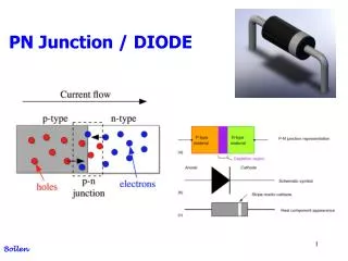
Diodes (The PN Junction) • If a piece of intrinsic silicon is doped so that half is n-type and the other half is p-type, a pn junction forms between the two regions as indicated in on the first slide • The p region has many holes (majority carriers) from the impurity atoms and only a few thermally generated free electrons (minority carriers). • The n region has many free electrons (majority carriers) from the impurity atoms and only a few thermally generated holes (minority carriers).
Diodes (The PN Junction) The free electrons in the n region are randomly drifting in all directions. At the instant of the pn junction formation, the free electrons near the junction in the n region begin to diffuse across the junction into the p region where they combine with holes near the junction. The same is true for the p-type material.
Diodes (The Depletion Region) When the pn junction is formed, the n region loses free electrons as they diffuse across the junction. This creates a layer of positive charges (ions) near the junction. As the electrons move across the junction, the p region loses holes as the electrons and holes combine. This creates a layer of negative charges (ions) near the junction. These two layers of positive and negative charges form the depletion region.
Diodes (The Barrier Potential ) • Any time there is a positive charge and a negative charge near each other, there is a force acting on the charges. • In the depletion region there are many positive charges and many negative charges on opposite sides of the pn junction. • The forces between the opposite charges form an electric field. • This electric field is a barrier to the free electrons in the n region, and energy must be expended to move an electron through the electric field. • That is, external energy must be applied to get the electrons to move across the barrier of the electric field in the depletion region.
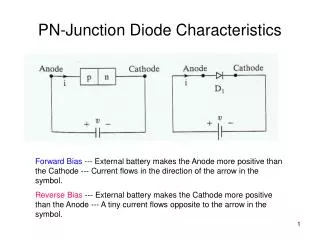
Diodes (Forward Bias ) • To bias a pn junction, apply an external dc voltage across it. Forward bias is the condition that allows current through a pn junction. The picture shows a dc voltage source connected by conductive material (contacts and wire) across a pn junction in the direction to produce forward bias. • This external bias voltage is designated as VBIAS. Notice that the negative side of VBIAS is connected to the n region of the pn junction and the positive side is connected to the p region. This is one requirement for forward bias. A second requirement is that the bias voltage, VBIAS, must be greater than the barrier potential (0.7V in silicon and 0.3 in germanium).
Diodes (Forward Bias ) Because like charges repel, the negative side of the bias-voltage source "pushes" the free electrons, which are the majority carriers in the n region, toward the pn junction. This flow of free electrons is called electron current. The negative side of the source also provides a continuous flow of electrons through the external connection (conductor) and into the n region as shown.
Diodes (Forward Bias ) • Since unlike charges attract, the positive side of the bias-voltage source attracts the electrons from the N-Region into the P-Region. • The holes in the P-Region provides a medium for electrons to move through the P-Region. The electrons move from hole to hole on to the left. • As they move they leave holes behind. The holes ellectively not actually move towards the pn junction. • This is called hole current.
Effect of Forward Bias on the Depletion Region • As more electrons flow into the depletion region, the number of positive ions is reduced. • As more holes effectively flow into the depletion region on the other side of the pn junction, the number of negative ions is reduced. • This reduction in positive and negative ions during forward bias causes the depletion region to narrow.
Effect of the Barrier Potential During Forward Bias • When forward bias is applied, the free electrons are provided with enough energy from the bias-voltage source to overcome the barrier potential and effectively move and cross the depletion region. • The energy that the electrons require in order to pass through the depletion region is equal to the barrier potential. In other words, the electrons give up an amount of energy equivalent to the barrier potential when they cross the depletion region. • This energy loss results in a voltage drop across the pn junction (0.7 for silicon and 0.3 for germanium). • An ideal diode does not have a barrier potential.
Characteristic curve for forward bias Very little current will flow until the bias voltage passes the value for the potential barrier
Characteristic curve for reverse bias • Diodes are not designed to allow current to flow in reverse bias. • Under high voltages the diode will break down and start conducting in reverse bias. • This voltage if called the break down voltage VBR • The diode at this point is no longer of any use as it cannot conduct current in only one direction any more.