Download
1 / 1
40 likes | 284 Views
Graphene p-n Junction. Daniel C. Ralph, Cornell University, ECCS - 0335765.

E N D
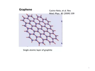
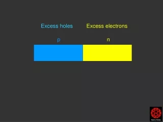
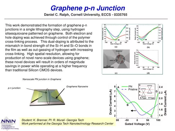
Graphene p-n Junction Daniel C. Ralph, Cornell University, ECCS - 0335765 This work demonstrated the formation of graphene p-n junctions in a single lithography step, using hydrogen silsesquioxane patterned on graphene. Both electron and hole doping was achieved through control of the polymer cross-linking process. This dual-doping is attributed to the mismatch in bond strength of the Si–H and Si–O bonds in the film as well as out-gassing of hydrogen with increasing cross-linking. High spatial resolution, allowing for production of novel nano-scale devices using graphene; these novel devices will result in orders of magnitude savings in power while operating at a higher frequency than traditional Silicon CMOS devices. Nanoscale PN junction in Graphene GrapheneNanowire p-n junction Student: K. Brenner, PI: R. Murali- Georgia Tech Work performed at the Georgia Tech Nanotechnology Research Center