Download
1 / 15
150 likes | 236 Views
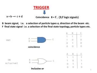
Trigger Interface and Distribution. 1. What is TID 2. TID Structure and functions 3. Possible usage in the system 4. TID related boards ( Mezz and FANIO) 5. Status. J. William Gu Jefferson Lab. 1. What is TID. V M E. T I D. T I D. T I D. T I D. T I D. T I D. T I D. T

E N D
Trigger Interface and Distribution 1. What is TID 2. TID Structure and functions 3. Possible usage in the system 4. TID related boards (Mezz and FANIO) 5. Status J. William Gu Jefferson Lab
1. What is TID V M E T ID T ID T ID T ID T ID T ID T ID T ID SD T ID T ID T ID T ID T ID T ID T ID T ID TS V M E ADC/TDC ADC/TDC ADC/TDC ADC/TDC ADC/TDC ADC/TDC ADC/TDC ADC/TDC CTP SD ADC/TDC ADC/TDC ADC/TDC ADC/TDC ADC/TDC ADC/TDC ADC/TDC ADC/TDC T ID V M E ADC/TDC ADC/TDC ADC/TDC ADC/TDC ADC/TDC ADC/TDC ADC/TDC ADC/TDC CTP SD ADC/TDC ADC/TDC ADC/TDC ADC/TDC ADC/TDC ADC/TDC ADC/TDC ADC/TDC T ID Upto 127 front end crates Trigger Interface (TI) + trigger Distribution (TD) = TID TID has some Trigger Supervisor functions
2. TID Structure and functions VMEPROM (FPGA firmware) Emergency/remote re-programming TrgSv Rev. 2 interface Xilinx Virtex-5 LX30T-FG665 VME 64x Optical IO HFBR-7924 #1,#2,#3,#4, #5,#6,#7,#8 VXS P0 TD mode: from SD TI/TS mode: to SD One dedicated link for redundant data collection External I/O (trg, clk…) Trg/Clk/Syc outputs On row_C
2. TID Structure and functions HFBR_1 MC100LVEP111 HFBR_2 HFBR_3 2.1 Clock Distribution P0_SD_CLK_IN HFBR_4 HFBR_5 CLK_OSC MC100EP57 TID_SELECT HFBR_6 TS_CLK HFBR_7 SUBSYS_CLK HFBR_8 CLK250_1 External_In AD9510 CLK1_in SyncCLK CLKSEL[1:0] CLK2AD CLK2AD CLK2_in CLKFPGAR CLK250_2 P0_CLKA ON_NB4N840 & SY55857 CLK125 P0_CLKC CLKFPGA SY58607 CLK250_P2 ASEL[1:0] CLK250_3 CLKTDC_P2 CLKTDC CLK_FREQ1 P0_CLKB CLK3125 CLKADC_P2 P0_CLKD CLK_FREQ2 CLKADC BSEL[1:0]
2. TID Structure and functions MC100LVEP14 HFBR#5 2.2 TD mode, trigger fanout HFBR#6 P0 SD_TRG_IN ADN2805 SY58607 HFBR#7 HFBR#8 Sel3 GTP#5_TX FPGA MC100LVEP14 HFBR#1 Front Panel HFBR#2 Ex_TRG_IN GTP#5_RX GTP#1_TX HFBR#3 HFBR#4 GTP#1_RX Mezz. (Rev2) TS2_TRG_IN Sel2 MC100LVEP14 TRG1A GTP#3_TX TRG1B P2_TRG1 FPGA_TRIG_1 F1_TRG FADC_TRG Sel1
2. TID Structure and functions HFBR-7934 #1 RX TX GTP connection details: All the eight fibers are connected to the FPGA, they are status input and trigger output in TD mode; and trigger input and status output in TI mode. (different FPGA firmware) FPGA XC5VLX30T GTP#1 MC100EP14 GTP#2 GTP#3 HFBR-7934 #4 GTP#4 RX TX GTP#5 GTP#6 GTP#7 GTP#8 HFBR-7934 #5 RX TX MC100EP14 TRIG1 TRIG2 WARNING/BUSY HFBR-7934 #8 RX TX TS_SD_P0_FAN_IN MC100EP11
2. TID Structure and functions 2.3 Sync signal distribution The encoding/decoding is implemented in the FPGA, synchronized to the 250MHz clock MC100EP14 P0_SyncA SEL TD_CLKSYNC I_delay Manchester decoding Sync decoding P0_SyncB P2_Sync FP_Sync1 Ext_Sync Encoding Mux O_delay FP_Sync2 MC100LVEP111 P0_CLKSYNC I_delay Manchester encoding O_delay HFBR7924#1 HFBR7924#2 FPGA HFBR7924#8
2. TID Structure and functions Trigger synchronization on trigger interface using SYNC signal A FIFO (built in the FPGA) is used to compensate for the DES. latency WORD 5 WORD 4 WORD 3 WORD 2 WORD 8 WORD 7 FIFO 1 WORD 1 WORD 0 WORD 6 Fiber 1T HFBR Fiber 1R HFBR Des. WORD 11 WORD 10 WORD 9 T-WORD 14 T-WORD 13 T-WORD 12 Ser FIFO n WORD 5 WORD 1 WORD 0 Fiber nT HFBR Fiber nR HFBR Des. WORD 4 WORD 3 WORD 2 WORD 8 WORD 7 WORD 6
2. TID Structure and functions 2.4 Front panel: The front panel will look like the drawing at the right. There are eight optical transceivers in TD mode, and one (or two) optical transceivers plus copper cable connectors in TI mode. 2.5 Other features: (always availableTM ) VME remote loading firmware; Serial links to switch slot#A, switch slot#B; Potential fast data link to SD;
3. Possible usage in the system 3.1 Standard experiment setup: This is the same content drawing as in page 2 Front End Readout Crate Trg/Clk/Sync ADC/TDC BUSY Trg/Clk/Sync TID1 Trg/Clk/Sync TID1 Trg/Clk/Sync SD BUSY BUSY BUSY ADC/TDC TID2 TID2 Up to 16 ADC/TDC Up to 8 TS SD TID8 Trg/Clk/Sync One Distribution Crate; Up to 127 Front End Crate, Plus the global trigger crate. BUSY Up to 16 TID16 TID Boards Global Trigger Distribution Crate
3. Possible usage in the system 3.2 Commissioning/testing setup (or a small DAQ system) Up to 9 (front end) crates in total Front End Crates V M E ADC/TDC ADC/TDC ADC/TDC ADC/TDC ADC/TDC ADC/TDC ADC/TDC ADC/TDC SD ADC/TDC ADC/TDC ADC/TDC ADC/TDC ADC/TDC ADC/TDC ADC/TDC ADC/TDC T ID Front End Crate V M E ADC/TDC ADC/TDC ADC/TDC ADC/TDC ADC/TDC ADC/TDC ADC/TDC ADC/TDC SD ADC/TDC ADC/TDC ADC/TDC ADC/TDC ADC/TDC ADC/TDC ADC/TDC ADC/TDC T ID /TS Up to 8 crates TID as TI (this crate) and TD (up to 8 other crates) with TS function V M E ADC/TDC ADC/TDC ADC/TDC ADC/TDC ADC/TDC ADC/TDC ADC/TDC ADC/TDC SD ADC/TDC ADC/TDC ADC/TDC ADC/TDC ADC/TDC ADC/TDC ADC/TDC ADC/TDC T ID
3. Possible usage in the system 3.3 Luxury option: parallel subsystem and global control; doubling the number of optical transceivers (expensive) V M E T ID T ID T ID T ID T ID T ID T ID T ID SD T ID T ID T ID T ID T ID T ID T ID T ID TS Global Distribution Crate Up to 16 TIDs Front End Crates V M E ADC/TDC ADC/TDC ADC/TDC ADC/TDC ADC/TDC ADC/TDC ADC/TDC ADC/TDC SD ADC/TDC ADC/TDC ADC/TDC ADC/TDC ADC/TDC ADC/TDC ADC/TDC ADC/TDC T ID V M E ADC/TDC ADC/TDC ADC/TDC ADC/TDC ADC/TDC ADC/TDC ADC/TDC ADC/TDC SD ADC/TDC ADC/TDC ADC/TDC ADC/TDC ADC/TDC ADC/TDC ADC/TDC ADC/TDC T ID Up to 8 crates Up to 8 crates V M E ADC/TDC ADC/TDC ADC/TDC ADC/TDC ADC/TDC ADC/TDC ADC/TDC ADC/TDC SD ADC/TDC ADC/TDC ADC/TDC TID/TS ADC/TDC ADC/TDC ADC/TDC ADC/TDC T ID V M E ADC/TDC ADC/TDC ADC/TDC ADC/TDC TID/TS ADC/TDC ADC/TDC ADC/TDC SD ADC/TDC ADC/TDC ADC/TDC ADC/TDC ADC/TDC ADC/TDC ADC/TDC ADC/TDC T ID One global distribution crate, Up to 127 front end crates One TID/TS per subsystem with Up to 8 crates (It is not required for the subsystem to have its global inputs from the same TID)
4. TID related boards (Mezz and FANIO) 4.1 Mezzanine board for TS_Rev2 interface Same connector and jumpers, same component (different package type) as TI_rev2 board; With the Mezzanine board, this TID will behave like a TI_Rev2 board, to work with TS_rev2. Board size: 2¼” x 3¼” How many mezz. Boards do we need? _____
4. TID related boards (Mezz and FANIO) 4.2 Fan out board (VME sized board) for CAEN 1290 TDC #1#5 It fans out the TRIGGER, CLOCK (41.7MHz), RESET signals; It merges the BUSY signals (OR); It communicates with VME P2 connectors (with TID); It supports up to 16 CAEN TDCs; One 64-pin cable (on FANIO board) four 16-pin cables (on CAEN 1290) How many fanout boards do we need? ________ #2#6 #3#7 #4#8 #9#13 #10#14 VME P2 #11#15 #12#16
5. Status 4 pieces are manufactured, two PCBs are being assembled; Board test starts next week