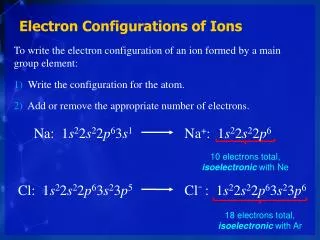
Download
1 / 31
340 likes | 612 Views
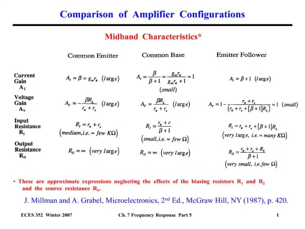
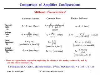
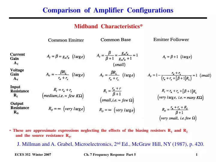
Comparison of Amplifier Configurations. Midband Characteristics*. These are approximate expressions neglecting the effects of the biasing resistors R 1 and R 2 and the source resistance R S.

E N D
Comparison of Amplifier Configurations Midband Characteristics* • These are approximate expressions neglecting the effects of the biasing resistors R1 and R2 • and the source resistance RS. J. Millman and A. Grabel, Microelectronics, 2nd Ed., McGraw Hill, NY (1987), p. 420. Ch. 7 Frequency Response Part 5
Characteristics of Amplifier Configurations Current gain is large ( β) for CE and EF, but < 1 for CB. Voltage gain is large for CE and CB, but < 1 for EF. • Input resistance is • Very small (few Ωs) for CB, • Medium (few KΩs) for CE, but • Very large (~ 10’s of KΩs) for EF. • Output resistance is • Very small (few Ωs) for EF, • Very large (~ 100’s of KΩs) for • CE and CB. Ch. 7 Frequency Response Part 5
Numerical Comparison of Amplifier Configurationsfor the Same Transistor and DC Biasing • These are approximate expressions neglecting the effects of the biasing resistors R1 and R2 • and the source resistance RS. Ch. 7 Frequency Response Part 5
Comparison of CB to CE Amplifier (with same Rs = 5 Ω) CE (with RS = 5 Ω) CB (with RS = 5Ω) Midband Gain Low Frequency Poles and Zeros High Frequency Poles and Zeroes Ch. 7 Frequency Response Part 5
Comparison of EF to CE Amplifier (For RS = 5Ω ) CE EF Midband Gain Low Frequency Poles and Zeros High Frequency Poles and Zeroes Ch. 7 Frequency Response Part 5
Comparison of Amplifier Configurations Midband Gain and High and Low Frequency Performance CE CB EF Midband Voltage Gain -191 V/V +102 V/V +0.987 V/V 45.6dB 40.2dB - 0.1dB Low 3dB Frequency 1.7x10⁴ rad/s 5.0x10⁴ rad/s 2.6x10² rad/s High 3dB Frequency 5.0x10⁷ rad/s 7.1x10⁸ rad/s 1.0x10¹⁰ rad/s RS= 5 Ω • Results for all three amplifiers with the smaller (5Ω) source resistance RS. Ch. 7 Frequency Response Part 5
Cascade Amplifier • Emitter Follower + Common Emitter (EF+CE) • Voltage gain from CE stage, gain of one for EF. • Low output resistance from EF provides a low source resistance for CE amplifier so good matching of output of EF to input of CE amplifier • High frequency response (3dB frequency) for Cascade Amplifier is improved over CE amplifier. CE EF Ch. 7 Frequency Response Part 5
Cascade Amplifier - DC analysis IB1 IB2 IE1 IRE1 Small Signal Parameters Ch. 7 Frequency Response Part 5
Cascade Amplifier - Midband Gain Analysis Note: rx1 = rx2 = 0 so equivalent circuit is simplified. Iπ1 + + Vπ1 _ + Vi Vπ2 _ _ Ri Note: Voltage gain is nearly equal to that of the CE stage, e.g. – 68 ! Ch. 7 Frequency Response Part 5
Cascade Amplifier - Low Frequency Poles and Zeroes • Use Gray-Searle (Short Circuit) Technique to find the poles. • Three low frequency poles • Equivalent resistance may depend on rπ for both transistors. • Find three low frequency zeroes. Ch. 7 Frequency Response Part 5
Cascade Amplifier - Analysis of Low Frequency PolesGray-Searle (Short Circuit) Technique Input coupling capacitor CC1 = 1 μF rπ1 Vπ1 + rπ2 RE1 Vπ2 _ IX Iπ1 Ri Vi RE1 rπ2 Ch. 7 Frequency Response Part 5
Cascade Amplifier - Analysis of Low Frequency PolesGray-Searle (Short Circuit) Technique CC2 rX2 Vo gm2Vπ2 Vπ2 RL rπ2 RC RE2 CE • Output coupling capacitor CC2 = 1 μF VX Vo RC RL Ch. 7 Frequency Response Part 5
Cascade Amplifier - Analysis of Low Frequency PolesGray-Searle (Short Circuit) Technique Emitter bypass capacitor CE = 47 μF Iπ1 gm1Vπ1 rπ1 Vπ1 VE1 Ie1 Iπ2 re1 Vπ2 gm2Vπ2 rπ2 RE1 VE2 Ix Ie2 re2 RE2 VX IE2 Low 3 dB Frequency The pole for CE is the largest and therefore the most important in determining the low 3 dB frequency. Ch. 7 Frequency Response Part 5
Cascade Amplifier - Low Frequency Zeros • What are the zeros for the Cascade amplifier? • For CC1 and CC2 , we get zeros at ω = 0 since ZC = 1 / jωC and these capacitors are in the signal line, i.e. ZC at ω = 0 so Vo 0. • Consider RE in parallel with CE • Impedance given by • When Z’E , Iπ 0, so gmVπ 0, so Vo 0 • Z’E when s = - 1 / RE2CE so pole for CE is at Ch. 7 Frequency Response Part 5
Cascade Amplifier - High Frequency Poles and Zeroes • Use Gray-Searle (Open Circuit) Technique to find the poles. • Four high frequency poles • Equivalent resistance may depend on rπ for both transistors. • Find four high frequency zeroes. High Frequency Equivalent Circuit Ch. 7 Frequency Response Part 5
Cascade Amplifier - High Frequency Poles Pole for Capacitor Cπ1 = 13.9 pF Ix + _ VX Ix- Iπ1 Iπ1 Ie1 Ch. 7 Frequency Response Part 5
Cascade Amplifier - High Frequency Poles Pole for Capacitor Cμ1 = 2 pF + _ Ix Iπ1 Ix- Iπ1 VX Ie1 Ch. 7 Frequency Response Part 5
Cascade Amplifier - High Frequency Poles and Zeroes Simplified Equivalent Circuit Using Miller’s Theorem, replace Cμ2 by two capacitors. Ch. 7 Frequency Response Part 5
Cascade Amplifier - High Frequency Poles Pole for Capacitor CT = 152 pF + _ Iπ1 Vπ1 Ve1 Ie1 Ix re1 VX Pole for Output Capacitor Cμ2 = 2 pF + VX gm2Vπ2 _ Ch. 7 Frequency Response Part 5
Cascade Amplifier - High Frequency Zeroes • When does Vo = 0? • When ω→∞, ZCμ1→ 0, so signal shorted to ground. ωZH1= ∞. • When ω→∞, ZCπ2→ 0, so rπ2 shorted, so Vπ2 = 0. ωZH2= ∞. • For Cπ1 , we get a zero when Ie1 = 0. Ie1 Ie1 Ch. 7 Frequency Response Part 5
Cascade Amplifier - High Frequency Zeroes • When does Cμ2 produce a zero, i.e. make Vo = 0? • For Cμ2 , we get a zero when IRL’ = 0, or ICμ2 = gm2Vπ2 , i.e. the output load resistance RL’ is starved of any current. I Cμ2 IRL’= 0 Zero for Output Capacitor Cμ2 = 2 pF Ch. 7 Frequency Response Part 5
Cascade Amplifier - High Frequency Poles and Zeroes Ch. 7 Frequency Response Part 5
Comparison of Cascade to CE Amplifier CE* Cascade (EF+CE) 2 X improvement in voltage gain ! Midband Gain Low Frequency Poles and Zeros High Frequency Poles and Zeroes 25 X improvement in bandwidth ! Ch. 7 Frequency Response Part 5 * CE stage with same transistor, biasing resistors, source resistance and load as cascade.
Comparison of Cascade to CE Amplifier • Why the better voltage gain for the cascade? • Emitter follower gives no voltage gain! • Cascade has better matching with source than CE. • Cascade amplifier has an input resistance that is higher due to EF first stage. • Versus Ri2 = rπ2 = 2.5 K for CE • So less loss in voltage divider term (Vi / Vs ) with the source resistance. • 0.91 for cascade vs 0.37 for CE. • Why better bandwidth? • Low output resistance re1 of EF stage gives smaller effective source resistance for CE stage and higher frequency for dominant pole due to CT (including Cμ2) Ri1 Ri2 Pole for Capacitor CT = 152 pF re1 Ch. 7 Frequency Response Part 5
Another Useful Amplifier – Cascode (CE+CB) Amplifier • Common Emitter + Common Base (CE + CB) configuration • Voltage gain from both stages • Low input resistance from second CB stage provides first stage CE with low load resistance so Miller Effect multiplication of Cμ1 is much smaller. • High frequency response dramatically improved (3 dB frequency increased). • Bandwidth is much improved (~130 X). Large Miller Effect Small Miller Effect Bandwidth is improved by a factor of 130X over that for the CE amplifier ! Ch. 7 Frequency Response Part 5
Example of Cascode (CE +CB) Amplifier http://www.freescale.com ECTW Conf. Proceedings 2003. Ch. 7 Frequency Response Part 5
Other Examples of Multistage Amplifiers CE CE EF EF Darlington Pair Ch. 7 Frequency Response Part 5
Other Examples of Multistage Amplifiers Push – Pull Amplifier Amplifier with Npn and Pnp Transistors Amplifier with FETs and Bipolar Transistors Ch. 7 Frequency Response Part 5
Differential Amplifier • Similar to CE amplifier, but two CE’s operated in parallel • Signal applied between two equivalent inputs instead of between one input and ground • Common emitter resistor or current source used • Current shared or switched between two transistors (they compete) • Analyze using equivalent half-circuit • 1/2 of signal at input • 1/2 of signal at output • 1/2 of source resistance • Gain and frequency response similar to CE amplifier for high frequencies • Advantage: • Rejects common noise pickup on input • No coupling capacitors so can operate down to zero frequency. _ + Vo Ch. 7 Frequency Response Part 5
Differential Amplifier Analysis Midband Gain Vo Vo /2 Low Frequency Poles and Zeros * Direct coupled so no coupling capacitors and no emitter bypass capacitor * No low frequency poles and zeros * Flat (frequency independent) gain down to zero frequency High Frequency Poles and Zeros Vo /2 Dominant pole using Miller’s Thoerem High frequency performance is very similar to CE amplifier. Ch. 7 Frequency Response Part 5
Summary • In this chapter we have shown how to analyze the high and low frequency dependence of the gain for an amplifier. • Analyzed the effects of the coupling capacitors on the lowfrequency response • Found the expressions for the corresponding poles and zeros. • Demonstrated Bode plots of magnitude and phase. • Analyzed the effects of the capacitances within the transistor on the highfrequency response. • Found the expressions for the corresponding poles and zeros. • Demonstrated Bode plots of the magnitude and phase. • Analyzed the high and low frequency performance of the three bipolar transistor amplifiers: common emitter, common base and emitter follower. • Found the expressions for the corresponding poles and zeros. • Demonstrated Bode plots of the magnitude and phase. • Demonstrated how to find the expressions for the gain and the high and low frequency poles and zeros for multistage amplifiers. Ch. 7 Frequency Response Part 5