Download
1 / 27
280 likes | 410 Views
Spectral properties of array sensors. Achim Gandorfer Tel. 397 room: S 2.82 email: gandorfer@linmpi.mpg.de. Outline. spectral range of CCDs limitations expanding the sensitivity range to the UV backside illumination deep depletion open electrode structure. Infrared sensors

E N D
Spectral properties of array sensors Achim Gandorfer Tel. 397 room: S 2.82 email: gandorfer@linmpi.mpg.de
Outline • spectral range of CCDs • limitations • expanding the sensitivity range to the UV • backside illumination • deep depletion • open electrode structure
Infrared sensors • choice of materials • sensor architecture • Hybrid detectors • flip-chip technique
Quantum efficiency • QE=Nel/Nph • depends on • wavelength • material • internal electric fields • sensor architecture
QE of silicon CCD • red limit: band gap of Si: 1.12 eV corresponds to λ=1.1 μm • blue limit: not intrinsic, due to surface structure! • transparency of electrodes decreases • reflection losses increase
Thick Front-side Illuminated CCD Incoming photons p-type silicon n-type silicon Silicon dioxide insulating layer 625mm Polysilicon electrodes These are cheap to produceusing conventional wafer fabrication techniques. They have a low Quantum Efficiency due to the reflection and absorption of light in the surface electrodes. Very poor blue response. The electrode structure prevents the use of an Anti-reflective coating that would otherwise boost performance. (stolen from: http://www.ing.iac.es/%7Esmt/CCD_Primer/CCD_Primer.htm )
15mm Thinned Back-side Illuminated CCD Anti-reflective (AR) coating Incoming photons p-type silicon n-type silicon Silicon dioxide insulating layer Polysilicon electrodes The silicon is chemically etched and polished down to a thickness of about 15microns. Light enters from the rear and so the electrodes do not obstruct the photons. The QE can approach 100% . These are very expensive to produce since the thinning is a non-standard process that reduces the chip yield. These thinned CCDs become transparent to near infra-red light and the red response is poor. Response can be boosted by the application of an anti-reflective coating on the thinned rear-side. These coatings do not work so well for thick CCDs due to the surface bumps created by the surface electrodes. Almost all Astronomical CCDs are Thinned and Backside Illuminated.
nt-ni nt+ni Anti-Reflection Coatings 1 Silicon has a very high Refractive Index (denoted by n). This means that photons are strongly reflected from its surface. [ ] 2 ni Fraction of photons reflected at the interface between two media of differing refractive indices = nt n of air or vacuum is 1.0, glass is 1.46, water is 1.33, Silicon is 3.6. Using the above equation we can show that window glass in air reflects 3.5% and silicon in air reflects 32%. Unless we take steps to eliminate this reflected portion, then a silicon CCD will at best only detect 2 out of every 3 photons. The solution is to deposit a thin layer of a transparent dielectric material on the surface of the CCD. The refractive index of this material should be between that of silicon and air, and it should have an optical thickness = 1/4 wavelength of light. The question now is what wavelength should we choose, since we are interested in a wide range of colours. Typically 550nm is chosen, which is close to the middle of the optical spectrum.
[ ] 2 ntx ni-ns 2 ntx ni+ns 2 ns nt 2 = Anti-Reflection Coatings 2 With an Anti-reflective coating we now have three mediums to consider : ni Air ns AR Coating nt Silicon The reflected portion is now reduced to : In the case where the reflectivity actually falls to zero! For silicon we require a material with n= 1.9, fortunately such a material exists, it is Hafnium Dioxide. It is regularly used to coat astronomical CCDs.
Anti-Reflection Coatings 3 The graph below shows the reflectivity of an EEV 42-80 CCD. These thinned CCDs were designed for a maximum blue response and it has an anti-reflective coating optimised to work at 400nm. At this wavelength the reflectivity falls to approximately 1%.
Quantum Efficiency Comparison The graph below compares the quantum of efficiency of a thick frontside illuminated CCD and a thin backside illuminated CCD.
‘Internal’ Quantum Efficiency If we take into account the reflectivity losses at the surface of a CCD we can produce a graph showing the ‘internal QE’ : the fraction of the photons that enter the CCDs bulk that actually produce a detected photo-electron. This fraction is remarkably high for a thinned CCD. For the EEV 42-80 CCD, shown below, it is greater than 85% across the full visible spectrum. Todays CCDs are very close to being ideal visible light detectors!
Electric potential Electric potential Potential along this line shown in graph above. Deep Depletion CCDs 1. The electric field structure in a CCD defines to a large degree its Quantum Efficiency (QE). Consider first a thick frontside illuminated CCD, which has a poor QE. Cross section through a thick frontside illuminated CCD In this region the electric potential gradient is fairly low i.e. the electric field is low. Any photo-electrons created in the region of low electric field stand a much higher chance of recombination and loss. There is only a weak external field to sweep apart the photo-electron and the hole it leaves behind.
Deep Depletion CCDs 2. In a thinned CCD , the field free region is simply etched away. Cross section through a thinned CCD Electric potential Electric potential There is now a high electric field throughout the full depth of the CCD. This volume is etched away during manufacture Red photons can now pass right through the CCD. Photo-electrons created anywhere throughout the depth of the device will now be detected. Thinning is normally essential with backside illuminated CCDs if good blue response is required. Most blue photo-electrons are created within a few nanometers of the surface and if this region is field free, there will be no blue response.
Deep Depletion CCDs 2. In a thinned CCD , the field free region is simply etched away. Cross section through a thinned CCD Electric potential Electric potential There is now a high electric field throughout the full depth of the CCD. Problem : Thinned CCDs may have good blue response but they become transparent at longer wavelengths; the red response suffers. This volume is etched away during manufacture Red photons can now pass right through the CCD. Photo-electrons created anywhere throughout the depth of the device will now be detected. Thinning is normally essential with backside illuminated CCDs if good blue response is required. Most blue photo-electrons are created within a few nanometers of the surface and if this region is field free, there will be no blue response.
Deep Depletion CCDs 3. Ideally we require all the benefits of a thinned CCD plus an improved red response. The solution is to use a CCD with an intermediate thickness of about 40mm constructed from Hi-Resistivity silicon. The increased thickness makes the device opaque to red photons. The use of Hi-Resistivity silicon means that there are no field free regions despite the greater thickness. Cross section through a Deep Depletion CCD Electric potential Electric potential Problem : Hi resistivity silicon contains much lower impurity levels than normal. Very few wafer fabrication factories commonly use this material and deep depletion CCDs have to be designed and made to order. Red photons are now absorbed in the thicker bulk of the device. There is now a high electric field throughout the full depth of the CCD. CCDs manufactured in this way are known as Deep depletion CCDs. The name implies that the region of high electric field, also known as the ‘depletion zone’ extends deeply into the device.
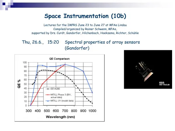
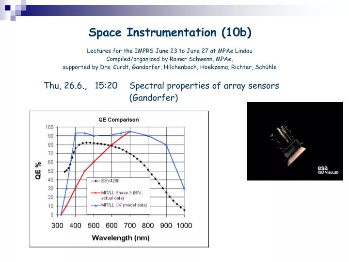
Deep Depletion CCDs 4. The graph below shows the improved QE response available from a deep depletion CCD. The black curve represents a normal thinned backside illuminated CCD. The Red curve is actual data from a deep depletion chip manufactured by MIT Lincoln Labs. This latter chip is still under development.The blue curve suggests what QE improvements could eventually be realised in the blue end of the spectrum once the process has been perfected.
Etaloning Another problem commonly encountered with thinned CCDs is ‘fringing’(also known as etaloning´. Etaloning is greatly reduced in deep depletion CCDs. Fringing is caused by multiple reflections inside the CCD. At longer wavelengths, where thinned chips start to become transparent, light can penetrate through and be reflected from the rear surface. It then interferes with light entering for the first time. This can give rise to constructive and destructive interference and a series of fringes where there are minor differences in the chip thickness. The image below shows some fringes from an EEV42-80 thinned CCD For spectroscopic applications, fringing can render some thinned CCDs unusable, even those that have quite respectable QEs in the red. Thicker deep depletion CCDs , which have a much lower degree of internal reflection and much lower fringing are preferred by astronomers for spectroscopy.
Open electrode structure • ring shaped electrodes on thick frontside illuminated CCD
Infrared Detector Technology • Which material?
Hybrid detectors photosensitive substrate + Silicon read-out circuit = hybrid detector
Substrate • array of n-p-photodiodes made from HgCdTe (epitactically grown on transparent carrier (CdZnTe/CdTe, Al2O3/CdTe (Sapphire)) • Boron implants to define pixel structure • Gold contacts on each pixel
read-out circuit (ROIC) • silicon based integrated circuit (CMOS array) with individually adressable pixels
„flip-chip-technique“ • substrate and ROIC are electrically connected pixel by pixel • Indium bumps