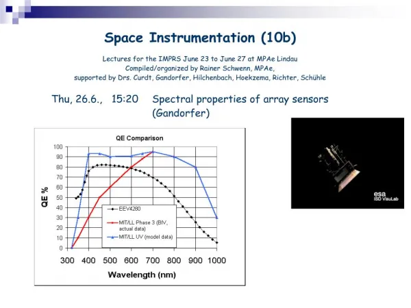
Download
1 / 20
200 likes | 337 Views
Investigation of properties of diamond sensors. K. Afanaciev, D. Drachenberg, E. Kouznetsova, W. Lange, W. Lohmann. Diamond samples. Fraunhofer Institute (Freiburg) : CVD diamond 12 x 12 mm 300 and 200 um thickness Different surface treatment : #1 – substrate side polished; 300 um

E N D
Investigation of properties of diamond sensors K. Afanaciev, D. Drachenberg, E. Kouznetsova, W. Lange, W. Lohmann
Diamond samples • Fraunhofer Institute (Freiburg) : • CVD diamond 12 x 12 mm • 300 and 200 um thickness • Different surface treatment : • #1 – substrate side polished; 300 um • #2 – substrate removed; 200 um • #3 – growth side polished; 300 um • #4 – both sides polished; 300 um • Metallization: • 10 nm Ti + 400 nm Au • Area 10 X 10 mm
HV Diamond Keithley 487 N2 I(V) dependence – setup Measurements were done with Keithly 487 picoammeter • Extremely low currents => • N2 atmosphere • EM shielding Reproducibility: measurements were done on different days with the same time regime
I(V) dependence Time dependence : => Very long setting time after bias voltage application: To perform measurements in a reasonable amount of time all the data were taken after 5 minutes of setting time
a I(V) dependence - results Usual I(V) curve: Non-ohmic curve: b 9 samples show this behavior Current is much higher here Hysteresis is probably due to polarization effect 3 samples from 3 different groups show this behavior
I(V) dependence – resistance • Average resistance ~(1013-1014) Ohm (ohmic behavior) • Different I(V) behaviors were observed even within groups with the same surface treatment • I(t) dependence shows hysteresis of the I(V) curves
ADC Sr90 PA delay diamond Scint. discr & PM1 Gate discr PM2 Charge Collection Distance (CCD) - Setup Qmeas. = Qcreated x ccd / L Qcreated(um)= 36 e-h pairs Trigger signal is taken from the scintillator. The scintillator is smaller than diamond so we could safely assume that triggering particles cross the diamond. • The samples haven’t been irradiated before this measurments • All data was taken 2 minutes after bias voltage applied
b a • Figure . Mean value of the signal from diamond in ADC channels versus voltage applied (on the top) and evaluated CCD versus field strength (on the bottom) for two different samples (a and b). CCD – dependence on bias voltage CCD dependence on voltage for different samples (groups 3 and 2) Top plots are in ADC channels and bottom in CCD The dependence is a bit different for ramping the voltage up and down Saturation is observed with fields in the order of 1-2 V per micron
CCD - results • #1 – substrate side polished; 300 um • #2 – substrate removed; 200 um • #3 – growth side polished; 300 um • #4 – both sides polished; 300 um • Not irradiated samples • Data were taken in the same time regime
CCD – irradiation studies The samples were irradiated with Sr-source with estimated dose-rate of about 0.45 Gray per hour Bias field was set to 1 V/m Irradiation was homogeneous over the sample area Noise and test pulse measurements were taken periodically to check the stability of electronics We were also monitoring current in the HV-circuit The total absorbed dose for all the samples was at least 5 Gy.
CCD – irradiation studies – results c Group #1 (substrate side polished). HV = 300V
CCD – irradiation studies – results b a Group #2 (substrate side cut, 200um). HV = 200V
CCD – irradiation studies – results Group #3 (growth side polished). HV = 300V
CCD – irradiation studies – results Group #4 (both sides polished). HV = 300V
CCD – irradiation studies – conclusions We have observed priming behavior (rise of ccd) for some of the samples (groups 2 and 1) For samples from group 3 we have observed extremely intense current growth (up to A) accompanied by noise growth and signal degradation Such a behavior was also observed for groups 1 and 4 but with less pronounced current growth and signal degradation There is no observable current growth in group #2 (cut substrate) There is also consistent increase in dark current of samples after irradiation It seems that surface treatment have considerable influence on sample behavior under irradiation -> GROUP#3 – to remove the substrate?
Reference spectra N (575) N (637) FAP 2_1 LO Phonon Si (770) FAP 4_2 Photoluminescence analysis HeCd Laser
Raman spectroscopy Result= S(diam)/S(graphite)*1000 Resolution ~ 1 cm-1
FAP 2_1 FAP 4_1 Raman spectroscopyresults
First NSC GPI diamonds • February 2004 – 2 diamond samples : • 250 and 350 um; 57 mm diameter • low (0.2 ppm) nitrogen contamination • Raman peak FWHM ~ 3 cm-1 • UV absorption spectra :