Download
1 / 39
410 likes | 536 Views
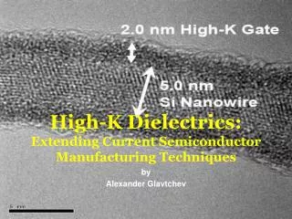
Ultrathin Gate Dielectrics on SiGe/SiGeC Heterolayers By Siddheswar Maikap Department of Physics Indian Institute of Technology (IIT), Kharagpur India. Who am I ?. IIT, Kharagpur, 1950 IIT, Kanpur, 1963 IIT, Bombay, 1958 IIT, Guwahati, 1994

E N D
Ultrathin Gate Dielectrics on SiGe/SiGeC Heterolayers By Siddheswar Maikap Department of Physics Indian Institute of Technology (IIT), Kharagpur India
Who am I ? IIT, Kharagpur, 1950 IIT, Kanpur, 1963 IIT, Bombay, 1958 IIT, Guwahati, 1994 IIT, Delhi, 1961 IIT, Roorkee, 2001 IIT, Madras, 1961
Ph.D Supervisors: Prof. S. K. Ray (Dept. of Physics) and Prof. C. K. Maiti (Dept. of E & ECE), IIT Kharagpur, IndiaJuly 1997 - October 2001 Postdoc Supervisors: Prof. Nong. M. Hwang and Prof. Doh. Y. Kim, Dept. of Material Science, Seoul National University, South Korea October 2001 - December 2002 Present Supervisor: Professor C. W. Liu, National Taiwan University, Taiwan 11th February 2003-
Outline of the Work • Introduction • Growth of group-IV alloy layers • Ultrathin oxides on partially strained layers • Extraction of material parameters for SiGe/SiGeC heterolayers • High-k gate dielectric for alternative SiO2 • Conclusion and Future work
Year 1998 2001 2004 2007 2010 Channel length (m) 0.2 0.14 0.1 <0.10 <0.07 Oxide thickness (nm) 4-6 4-5 4-5 <4 <4 Technology Roadmap Moore’s law: the gate length and cost production lines as a function time. Source: National Technology Roadmap for semicon-ductors, Semiconductor Industry Association, San Jose, USA, 1997 (After D. J. Paul, Adv. Mater., vol. 11, p. 191).
Requirements of gate quality ultrathin oxide High quality Si/SiO2 interface Low defect density Stability under hot carrier stress Low thermal budget Good barrier properties against impurity diffusion Reduced B-penetration from doped poly-Si gate
Why SiGe? • Band-gap engineered semiconductor devices for VLSI/ULSI technology • Enhancement of low field hole mobility: CMOS devices • Heterojunction bipolar transistor (HBT) for high speed digital and microwave circuits • Modulation doped field effect transistor (MODFET) • Quantum well detectors • Resonant tunneling diodes
Growth of Group-IV Alloy Layers on Si Schematic diagram of strained and relaxed epilayer on a Si substrate. In the relaxed layer, many dislocations are seen at the epi/substrate interface. According to Vegard’s rule: where, aSi=5.43Å, aGe=5.65Å and ac=3.57Å
Critical Layer Thickness Critical layer thickness of Si1-xGex films as a function of Ge mole fraction. Lines show theoretical kinetic model for various growth temperature. Figure is after D. C. Houghton et al., J. Appl. Phys., vol. 70, 1991, p. 2136.
Role of C in SiGe System • Strain compensation by substitutional C in SiGe: 1 at % C compensates 8.2-10 at % Ge • Possibility of SiGeC system with either compr- essive or tensile strain: Additional flexibility in strain & band-gap engineering • Better surface smoothness • Higher critical layer thickness • Higher strain relaxation temperature According to Vegard’s rule: where, aSi=5.43Å, aGe=5.65Å and ac=3.57Å
Strain Compensation Critical layer thickness of Si1-x-yGexCy as a function of Ge and C concentration. Figure is after Amour et al., Thin Solid Film., vol. 294, 1997, p. 112.
High Resolution X-ray Diffraction (004) HRXRD spectra from Si0.8Ge0.2 and Si0.69Ge0.3C0.01 films According to Vegard’s rule: where, aSi=5.43Å, aGe=5.65Å and ac=3.57Å
Sample Zrms (Å) Si0.6Ge0.4 22 Si0.56Ge0.4C0.04 1.3 Si0.74Ge0.26 7.58 Si0.69Ge0.3C0.01 11.8 Atomic Force Microscopy AFM (5 m x 5 m) scan of film surface. (a) Si0.6Ge0.4 sample (~22 Å rms), (b) Si0.56Ge0.4C0.04 sample (~1.3 Å rms).
Gate oxides on group-IV alloy layers • Problem in conventional thermal oxidation: • High temperature oxidation: Not suitable for • group-IV alloys due to strain relaxation • Selective oxidation of Si: Ge segregation and C precipitation • Misfit dislocations due to high temperature process • Degradation of mobility due to relaxed layer at • processing temperature • Solution: • Low temperature oxidation • Minimize the misfit dislocation
Low Thermal Budget Methods for Oxidation Rapid thermal oxidation (RTO) Low pressure chemical vapor deposition (LPCVD) Plasma oxidation Why Microwave Plasma Oxidation • Electrodeless, Low self bias and High ionization efficiency • Low temperature (<200oC) growth • Reduced impurity distribution • Absence of Ge segregation • Absence of C precipitation
Experimental Setup Schematic diagram of microwave discharge cavity system Oxidation time: 2 min Initial Pressure: 10-3 Torr Growth Pressure: 1.0 Torr Temperature: ~200oC Growth rate: 405 Å/min Refractive index: 1.44-1.46 (Ellipsometry)
High Resolution X-ray Diffraction High resolution X-ray diffraction characteristics for (a) as-grown, (b) plasma grown and (C) thermal (750oC, 100 min) oxides on Si0.685Ge0.3C0.015 samples.
Location of Different Trap Charges Location of trapped charges at different regions in the MOS structures.
Fixed Oxide Charge and Interface State Density where, A is the gate area, ms is the work function between metal and semiconductor, Gmax is the maximum conductance, is the angular frequency, and Cm is the capacitance at Gmax. C-V and G-V characteristics for plasma grown Si0.69Ge0.3C0.01 sample. Qf/q= -2.7x1011 cm-2 Dit= 5.4x1011 cm-2 eV-1
Extraction of Material Parameters of SiGe/SiGeC Heterolayers Hole confinement characteristics Extraction of Si-cap layer thickness Extraction of buried and surface channel threshold voltages Determination of valence band offset: Si1-xGex and Si1-x-yGexCy heterolayers Generation lifetime of group-IV alloy layers
Hole confinement characteristics High frequency (1 MHz) C-V characteristics of a MOS capacitor. Simulated HF and low frequency C-V characteristics are also shown.
Extraction of Si-cap Layer Thickness Apparent doping concentration vs. distance from the Si/SiO2 interface. Unconsumed Si-cap layer thickness: 30A
Extraction of Threshold Voltages 1-D numerical simulation of hole charge in buried channel (QH, SiGe) and in surface channel (Qs, Si-cap) as a function of gate voltage. Experimental apparent doping vs. gate voltage characteristics.
Effect of Ge Concentration SiGe-well Si-cap Low frequency C-V characteristics Hole concentration in Si-cap and SiGe-well
Extraction of Valence Band Offset (Ev) where, and where HPotential at top heterointerface FFermi potential THPotential at threshold at the top heterointerface tcapThickness of Si cap layer SiPermittivity of Si XdmMaximum depletion layer width VT=VTH-VTS, gate voltage window
Valence Band Offset: SiGe and SiGeC Summary of experimentally measured Ev in strained Si1-xGex and partially strain compensated Si1-x-yGexCy heterolayers.
Sample Doping (cm-3) g (s) <100> CZ Si (Schwartz et al.) 5x10¹⁵ 9 Control Si (this work) 5x10¹⁵ 5.6 Si0.82Ge0.18 (Schwartz et al.) 3x10¹⁷ 1.45 Si0.9Ge0.1 (Riley et al.) 2.5x10¹⁷ 2.6 Si0.8Ge0.2 (this work) 2x10¹⁷ 1.4 Si0.8Ge0.18C0.02 (Lippert et al.) 5x10¹⁷ 0.12 Si0.795Ge0.2C0.005 (this work) 2x10¹⁷ 1.2 Generation Lifetime in Si-based Heterolayers Transient response of capacitance-time plot for a partially strained Si0.795Ge0.2C0.005 MOS capacitor.
Why high-k dielectric ? Problem in conventional ultrathin SiO2 ( <2 nm): • High leakage current • Low breakdown field • Poor reliability Solution: • High-k dielectric as a gate material
Why ZrO2 andHfO2? J. Robertson, MRS Bull. March 217 (2002) High dielectric () constant: 17-30 Thermodynamically stable on Si High breakdown field: ~ 10-15 MV/cm Large band gap: 5 -8 eV Low leakage current
Vg Al ZrO2 /HfO2 Interfacial layer SiGe Deposition conditions of ZrO2 films on SiGe/SiGeC by RF magnetron sputtering Substrate temperature: 350oC Base pressure: 5x10⁻⁶ Torr Deposition pressure: 0.2 Torr Ar:O2: 4:1 Deposition time: 20 min RMS roughness: ~ 6.5 nm for 1hr ~ 8.0 nm for 1.5 hr
Glue ZrO2 ~ 8.5 nm IL ~ 3.9 nm Si0.69Ge0.3C0.01~ 40 nm Cox = 1116 pF Si epilayer
Interfacial layer ZrO2 with interfacial layer ZrO2 (k) ~ 17.5 IL (k) ~ 7.0 Effective k ~ 12.2 EOT ~ 3.9 nm 1/Ceq= 1/CZrO2+ 1/Cinterfacial layer teq= (3.9/kIL)tIL + (3.9/khigh-k)thigh-k
(a) (b) (c) Hf Hf Hf HfO HfO HfO N N HfSiO HfSiO HfSiO Ultra-thin HfO2 films on p-Si
H-related trap Substrate temperature: 350oC Base pressure: 5x10⁻⁶ Torr Deposition pressure: 13.5 mTorr Ar/N2 : 19 sccm: 7 sccm Deposition time: 3 min
Conclusion High quality strained Si1-xGex and partially strain compensated Si1-x-yGexCy heterolayers: UHVCVD Strained layer characterization: Composition and thickness of group-IV alloy layers: SIMS analysis Crystalline quality: HRXRD study Surface roughness: AFM study Low-temperature plasma oxidation: Preserve the strain in group-IV alloy layers
Extraction of material parameters for SiGe and SiGeC heterolayers: Threshold voltages of buried and surface channel, valence band offset, and carrier generation lifetime ZrO2 and HfO2 high-k gate dielectrics Physical characterization: HRTEM, ToF-SIMS, XPS and AES measurements Electrical characterization: C-V, G-V, I-V and gate voltage shift
Future scope Annealing effect on ZrO2 and HfO2 high-k dielectrics on Si, SiGe, SiGeC and strained-Si heterolayers Stacked gate dielectrics, NH3/HfO2 /N2O, on Si, SiGe, SiGeC and strained-Si heterolayers
Acknowledgments: The author is grateful to Professor S. K. Banerjee, The University of Texas at Austin, for providing experimental support for the growth of strained Si1-xGex and Si1-x-yGexCy samples used in this study. The authorgratefully acknowledge financial support from the Creative Research Initiatives Program of the Korea Ministry of Science and Technology, South Korea