Understanding RAM, ROM, and Programmable Logic Devices in Digital Logic Design
This chapter delves into the intricacies of Random-Access Memory (RAM) and Read-Only Memory (ROM) used in digital logic design. It covers data storage characteristics, memory locations, and address lines, exploring both volatile and non-volatile memory types. Additionally, the section highlights programmable logic devices (PLDs) including PROM, PAL, and PLA, explaining their structure and function in implementing Boolean functions. Through various examples, the reader will gain a solid understanding of memory organization, decoding, and programmable logic.


Understanding RAM, ROM, and Programmable Logic Devices in Digital Logic Design
E N D
Presentation Transcript
Chapter 7: Digital Logic Design Memory and Programmable Logic
Random-Access Memory (RAM) • Data Storage (Volatile) • Locations (Address) • Byte or Word Data input Memory unit 16 x 8 Address Read Write Data output
Random-Access Memory (RAM) • Data Storage (Volatile) • Locations (Address) • Byte or Word m Data input Memory unit 2k x m k Address Read 10 Address lines 1024 locations = 1 K Write m Data output
BC Memory Decoding • Memory Cell Select Output Input Read/Write
Input Data 0 I1 AddressLines BC BC BC BC BC BC BC BC BC BC BC BC BC BC BC BC I0 1 2 x 4Decoder 2 MemoryEnable E 3 Read/Write Output Data Memory Decoding • Memory Array
Read-Only Memory (ROM) ROM 2k x m k Address Memory Enable m Data output
Read-Only Memory (ROM) Conventional Symbol Array Logic Symbol
Read-Only Memory (ROM) • 8 x 4 ROM 3 x 8Decoder 0 1 2 I2 3 AddressLines I1 4 I0 5 6 MemoryEnable E 7 Output Data
Read-Only Memory (ROM) 3 x 8Decoder • 8 x 4 ROM 0 1 0 0 0 0 2 11 0 1 A2 I2 3 0 0 11 A1 I1 4 1 0 0 0 A0 I0 5 1111 6 1 0 0 1 E 1 7 0 111 0 0 0 0 D3 D2 D1 D0
Types of ROMs • Mask Programmed ROM • Programmed during manufacturing • Programmable Read-Only Memory (PROM) • Blow out fuses to produce ‘0’ • Erasable Programmable ROM (EPROM) • Erase all data by Ultra Violetexposure • Electrically Erasable PROM (EEPROM) • Erase the required data using an electrical signal
Programmable Logic Device (PLD) • Boolean Functions: • Sums-of-Products • AND-plane followed by OR-plane
Fixed AND array (Decoder) Programmable AND array Programmable AND array Programmable OR array Fixed OR array Programmable OR array Inputs Inputs Inputs Outputs Outputs Outputs Programmable Logic Device (PLD) • PROM • PAL • PLA
Programmable Array Logic (PAL) Example w(A,B,C,D)= ∑(2,12,13) x(A,B,C,D)= ∑(7,8,9,10,11,12,13,14,15) y(A,B,C,D)= ∑(0,2,3,4,5,6,7,8,10,11,15) z(A,B,C,D)= ∑(1,2,8,12,13) Simplify: w =ABC’ + A’B’CD’ x =A + BCD y =A’B + CD + B’D’ z =ABC’+ A’B’CD’ + AC’D’ + A’B’C’D = w + AC’D’+ A’B’C’D w A x B y C z D
Programmable Logic Array (PLA) A B C Example: F1=AB’ + AC + A’BC’ F2=(AC + BC)’
Sequential Programmable Logic Device • Basic Macrocell Logic
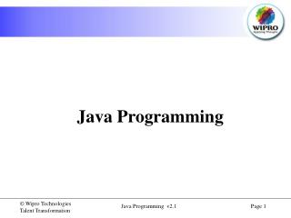
Homework • Mano • Chapter 7 • 7-1 • 7-2 • 7-3 • 7-18 • 7-19