Download
1 / 19
200 likes | 504 Views
What is the limit of nanolaminate layer thickness in ALD? Oskari Elomaa , 20.4.2010 . Nanolaminates by ALD: tailored properties & controlled growth! But are there limitations for the layer thickness?. Contents. Nanolaminates: introduction and examples Nanolaminates by ALD

E N D
What is the limit of nanolaminate layer thickness in ALD?OskariElomaa, 20.4.2010
Nanolaminates by ALD: tailored properties & controlled growth! But are there limitations for the layer thickness?
Contents • Nanolaminates: introduction and examples • Nanolaminates by ALD • Layer thickness limitations • Property related • Thick layers • Thin layers • Process and modelling examples • Conclusions • References
Nanolaminates: introduction Multilayer coatings • Repeating layers of different materials • One or more bilayers in a stack • Bilayer thickness from few to tens of nm Growthmethods • CVD • PVD • ALD • Sol-Gel Cross-sectional TEM image of Al2O3–TiO2 film nanolaminated by alternate ALD growth of 100-cycle Al2O3 and 350-cycle TiO2. [2] [1-5]
Nanolaminates: introduction Tunable nanocomposites • Materials (single layer properties), composition • Thickness and number of bilayers • Iso-structural vs. non iso-structural bilayers • Crystal sructure (polycrystalline, amorphous) Possibility to tailor the properties • High strenght and hardness • Corrosion/erosion resistance • Fracture toughness • High film quality (low roughness) • High/low thermal/electrical conduction • High/low optical refractive index [1-5]
Nanolaminates: examples Hardcoatings and highstrenghtmaterials • TiAlN/VN, TiAlN-CrN, AlN/Si3N4… • Machine tooling Thin high-k dielectric layers • Al2O3/HfO2, Ta2O5/HfO2, Ta2O5/ZrO2, ZrO2/HfO2... • Gate dielectric candidates to replace SiO2, SiON • Capasitor dielectrics Othertailoredmultilayercoatings • W/AI2O3… • Thermalbarriercoatings • Opticalfilters, x-raymirrors, gassensors [1-15]
Nanolaminates by ALD Basic ALD process • Precursors changed after each individual layer to get bilayers • 3 or more precursors ALD advantages compared to PVD, CVD... • Accurate thickness control • Large-scale uniformity • Conformal layering • Sharp interfaces • Diverse sizes and shapes can be coated ALD limitations • Speed (slow) • Precursors (none, toxic, expensive) [1, 5-6]
Limits of thickness 1: nanolaminate Critical thickness • Nanolaminate property (mechanical, elecrical etc.) related • Optimum bilayer thickness for spesific property • AlN/TiN hardness maximum when AlN 2 nm • TiO2 amorphous between 2,5 and 9 nm [8, 16-17]
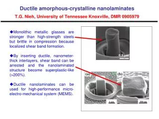
Limits of thickness 2: thick ALD Defects and imperfections multiply (in crystalline) • Surface roughness increases • Unwanted-wanted depending on application • Faceting increases • layers in the stack not parallel with the substrate • Stresses, cracks Some of the problems can be avoided by amorphous layer • crystalline/amorphous bilayernanolaminate • see example 1 [1, 5, 8]
ALD process: example 1 ZnO2/Al2O3 nanolaminates • ZnO polycrystalline electric conductor • Al2O3 amorphous insulator Process • Diethyl zinc (DEZ), trimethyl aluminum (TMA) and H2O • 1-128 bilayers • Deposited at 177 C [1]
ALD process: example 1 Results • Speed of growthsimilar to normal ALD • Surface roughness: from 6 to 0,2 • MinimumAl2O3 needed: one monolayer [1]
Limits of thickness 3: thin ALD Basicallymonolayerbymonolayerbut: • the surface is only gradually converted from into actual film • adsorption, limited number of reactive sites, • density of reactive sites on substrate and film Nucleation phenomena • islands • especially in polycrystalline films • can affect the growth (unperfect films) • W on Al2O3 limits the minimum thickness of a continuous W nanolayer to ~25Å [5-6,17-18]
ALD modelling : example 2 Hypothesis: • Reactant adsorption depends on properties of the surface and absorbant • The surface changes during the initial deposition from substrate to film • Difference between initial stage and the stabilized stage • Film thickness is not linearly dependent of cycles during the first few • The film thickness becomes linearly dependent After the initial cycles [17-18]
ALD modelling : example 2 Results [17-18]
Limits of thickness 3: process Chamber atmosphere • Optimum temperature/pressure window for each layer • No unwanted growth, thickness control Precursors • Temperature, dependence of the substrate • self-decomposition and residues need to be avoided Substrates • Oxide or stripped affects growth mode • Amorphous or crystalline (surface roughness limitations) Speed = time = money • ALD is slow to be economical (but batch processing) • Typically few nm/min [1, 5, 13-16]
Conclusions Nanolaminates by ALD: • Tailored properties (mechanical, electrical etc.) • Controlled growth, conformality • From thin gate oxides to thick tool coatings But layer thickness is limited by: • Critical thickness • Defects and imperfections • Surface roughness and faceting • Stresses (thermal, thickness related) • Non-linear growth in the beginning • Process parameters
THANK YOU FOR LISTENING! QUESTIONS?
References • 1: J.W. Elam, Z.A. Sechrist, S.M. George, ZnO/Al2O3 nanolaminates fabricated by atomic layer deposition: growth and surface roughness measurements, Thin Solid Films 414 (2002) 43–55 • 2: Yong Shin Kim, Sun Jin Yun, Nanolaminated Al2O3–TiO2 thin films grown by atomic layer deposition, Journal of Crystal Growth 274 (2005) 585–593 • 3: Philip C. Yashar,William D. Sproul, Nanometer scale multilayered hard coatings, Vacuum 55 (1999) 179}190 • 4: Lijuan Zhong, Fang Chen, Stephen A. Campbell, and Wayne L. Gladfelter ,Nanolaminates of Zirconia and Silica Using Atomic Layer Deposition, Chem. Mater. 2004, 16, 1098-1103 • 5: Markku Leskelä, Industrial Applications of Atomic Layer Deposition (ALD), 10th MIICS Conference • Mikkeli, March 18, 2010 • 6: J. M. Jensen, A. B. Oelkers, R. Toivola, and D. C. Johnson, X-ray Reflectivity Characterization of ZnO/Al2O3Multilayers Prepared by Atomic Layer Deposition, Chem. Mater. 2002, 14, 2276-2282 • 7: R. M. Costescu, D. G. Cahill, F. H. Fabreguette, Z. A. Sechrist, S. M. George, Ultra-Low Thermal Conductivity in W/Al2O3 Nanolaminates, Science 303, 989 (2004) • 8:, D.R.G. Mitchell*, D.J. Attard, K.S. Finnie, G. Triani, C.J. Barbe´, C. Depagne, J.R. Bartlett TEM and ellipsometry studies of nanolaminate oxide films prepared using atomic layer deposition, Applied Surface Science 243 (2005) 265–277 • 9: T.M. Mayer, T.W. Scharf, S.V. Prasad, N.R. Moody, R.S. Goeke, M.T. Dugger, R.K. • Grubbs, S. M. George, R.A. Wind, J.M. Jungk, W.W. Gerberich, Atomic Layer Deposition of Highly Conformal Tribological Coatings, SANDIA REPORT 2005 • 10: Dr. Troy Barbee, Optical applications of nano-laminates, Technology Days in the Government • Mirror Development and Related Technologies
References • 11: Diana Riihelä, Mikko Ritala , Raija Matero, Markku Leskelä, Electronics, Optics and Opto-electronics, Introducing atomic layer epitaxy for the deposition of optical thin films, Thin Solid Films 289 (1996) 250-255 • 12: H. Zhang and R. Solankia, B. Roberds, G. Bai, and I. Banerjee, High permittivity thin film nanolaminates, JOURNAL OF APPLIED PHYSICS 87 4 2000 • 13: Lijuan Zhong, Weston L. Daniel, Zhihong Zhang, Stephen A. Campbell, and Wayne L. Gladfelter • , Atomic Layer Deposition, Characterization, and Dielectric Properties of HfO2/SiO2 Nanolaminates and Comparisons with Their Homogeneous Mixtures. Chem. Vap. Deposition 2006, 12, 143–150 • 14: H. Zhang and R. Solankiz, Atomic Layer Deposition of High Dielectric Constant • Nanolaminates, Journal of The Electrochemical Society, 148 4 2001 • 15: Kijung Yong and Joonhee Jeong , Applications of Atomic Layer Chemical Vapor Deposition for the Processing of Nanolaminate Structures, Korean d. Chem. Eng., 19(3), 451-462 (2002) • 16: Steven M. George, Fabrication of Nanolaminates with Ultrathin Nanolayers Using Atomic Layer • Deposition: Nucleation & Growth Issues, AFOSR Grant No. FA9550-06-1-0075, Final Report 2009 • 17: Jung-Wook Lim, Hyung-Sang Park, and Sang-Won Kang, Kinetic Modeling of Film Growth Rate in Atomic Layer Deposition, Journal of The Electrochemical Society, 148 6 C403-C408 2001 • 18: Jung-Wook Lim, Hyung-Sang Park, and Sang-Won Kang, Analysis of a transient region during the initial stage of atomic layer deposition JOURNAL OF APPLIED PHYSICS 88 (11) 2000