Flash memories
Flash memories. Based on: Roberto Bez et al., ST Microelectronics Proceedings of the IEEE, Vol. 91 no. 4, April 2003. Contents. Non-volatile memories what are NVM method of operation EPROM, EEPROM, and Flash Reliability concerns retention endurance Scaling. Non-Volatile Memories.

Flash memories
E N D
Presentation Transcript
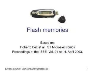
Flash memories Based on: Roberto Bez et al., ST Microelectronics Proceedings of the IEEE, Vol. 91 no. 4, April 2003.
Contents • Non-volatile memories • what are NVM • method of operation • EPROM, EEPROM, and Flash • Reliability concerns • retention • endurance • Scaling
Non-Volatile Memories • A non-volatile memory is a memory that can hold its information without the need for an external voltage supply. The data can be electrically cleared and rewritten • Examples: • Magnetic Core • Hard-disk • OTP: one-time programmable (diodes/fuses) • EPROM: electrically programmable ROM • EEPROM: electrically erasable and programmable ROM • Flash
IC memory classification Non-volatile memories Keep data without power supply Volatile memories Lose data when power down SRAM DRAM ROM PROM EPROM EEPROM Stand-alone versusembedded memories This lecture: stand-alone FLASH EEPROM
Non-volatile memory comparison Floating gate memories Comparison: later today
How does a Flash memory cell work? …How does a MOS transistor work? …What is a semiconductor? See: college Halfgeleiderdevices!!
Semiconductor essentials: properties • Metallic conductor: • typically 1 or 2 freely moving electrons per atom • Semiconductor: • typically 1 freely moving electron per 109-1017 atoms
Semiconductors in the periodic table Elemental semiconductors: C, Si, Ge (all group IV) Compound semiconductors: III-V: GaAs, GaN… II-VI: ZnO, ZnS,… Group-III and group-V atoms are “dopants”
Semiconductor essentials: impurities • Small impurities can dramatically change conductivity: • slight phosphorous contamination in silicon gives many extra free electrons in the material (one per P atom!) • slight aluminum contamination gives many extra holes (one per Al atom) P Al
Silicon dopants Boron most widely used as p-type dopant; Phosphorous and arsenic both used widely as n-type dopant
p-n junction: current can only flow one way! Semiconductor diode Semiconductor essentials: n and p type n-type doped semiconductor e.g. silicon with phosphorus impurity electrons determine conductivity p-type doped semiconductor e.g. silicon with Al impurity holes determine conductivity
- - - - depletion - - - - - - - - - - inversion The field effect + + + + + + + + accumulation
- - - - - - - - - - The MOS transistor - - - - - - - - - - SOURCE DRAIN
A MOS transistor layout source gate drain source gate drain (cross section) (top view) (cross section)
Free electron Free hole NMOS and PMOS transistors NMOS PMOS + + + - - - Conducts at +VGB Conducts at -VGB NMOS + PMOS = CMOS
Vfb VT depletion accumulation inversion MOSFET operation (very basic) C V
inversion Current through the MOS transistor Channel charge: Q ~ (Vgs – VT) Channel current: I ~ (Vgs – VT) MOS transistor - simplistic MOS transistor - real I I Vgs Vgs VT VT
Id Vgs Concept of the floating-gate memory cell • MOS transistor: 1 fixed threshold voltage • Flash memory cell: VT can be changed by program/erase MOS transistor Floating gate transistor Id programming erasing Vgs VT
Floating gate animation http://www3pub.amd.com/products/nvd/mirrorbit/flash.htm
Control gate Floating gate Floating gate transistor: principle • VT is shifted by injecting electrons into the floating gate; • It is shifted back by removing these electrons again. • CMOS compatible technology!
Channel charge in floating gate transistors unprogrammed programmed Control gate Control gate Floating gate Floating gate silicon To obtain the same channel charge, the programmed gate needs a higher control-gate voltage than the unprogrammed gate
Logic “0” and “1” Reading a bit means: 1. Apply Vread on the control gate 2. Measure drain current Id of the floating-gate transistor When cells are placed in a matrix: Id ΔVT = -Q/Cpp drain lines Vgs Vread Control gate lines “1” → Iread >> 0 “0” → Iread = 0
NOR NAND NOR or NAND addressing ‘Word’ = control gate; ‘bit’ = drain less contacts → more compact
NAND versus NOR 10x better endurance Fast read (~100 ns) Slow write (~10 μs) Used for Code Smaller cell size Slow read (~1 μs) Faster write (~1 μs) Used for Data
Control gate Floating gate SiO2 Si3N4 Polysilicon Programming and erasing the floating gate Control gate Floating gate
Program/erase of a floating gate transistor • Floating gate is surrounded by insulating material. • How to drive charge in and out of it? • Injection/ejection mechanisms: • Fowler-Nordheim tunneling (FN) • Channel Hot Electron Injection (CHE) • Irradiation (most common: UV, for EPROMs)
Conduction through SiO2 • Dominant current components: • Intrinsic quantummechanical conduction • Fowler-Nordheim tunneling • Direct Tunneling • Defect-related: • Trap-assisted tunneling (via a molecular defect) • Current through large defects(e.g. pinholes) • Intrinsic current is defined by geometry & materials • Defect-related current can be suppressed by engineering VG VD VB
Gate oxide conduction - example 4 nm oxide -3 10 -4 Hard 10 breakdown -5 10 -6 10 Soft breakdown -7 (A) 10 | -8 10 G I | -9 10 -10 10 -11 10 SILC -12 10 Unstressed oxide -13 10 -14 10 -2 -1 0 1 2 3 4 5 V (V) G
CHE: Hot electron programming Hot holes Hot electrons Field kinetic energy overcome the barrier Hole substrate current Pinch-off high electric fields near drain hot carrier injection through SiO2 Note: < 1% of the electrons will reach the floating gate power-inefficient
CHE: properties • Works only to create a positive VT shift • High power consumption: ~300 µA/cell(most electrons get to the drain: lost effort) • Moderate programming voltages • Risky: hot carriers can damage materials • May lead to fixed charge, interface traps, bulk traps • Results in degradation of the cell (see later)
Fowler-Nordheim tunneling • Uniform tunneling through entire dielectric is possible • VT-shift can be positive as well as negative Can be used for program and erase • Requires high voltage and high capacitances • Little power needed (~10 nA/cell) • Risks of this technique: • Charge trapping in oxide • Stress-induced leakage current • Defect-related oxide breakdown
Uniform or drain-side FN tunneling Non-uniform: only for erasing; less demanding for the dielectric
Alternative: tunnel through interpoly oxide • (erasing, combined with CHE program) • Less demanding for the tunnel oxide • Therefore less SILC and better retention • More demanding for interpoly oxide • Uses high voltage and low power
Flash reliability issues and scaling • Flash reliability concerns: • The regular reliability concerns of CMOS • Oxide breakdown • Interconnect problems (electromigration) • … • Specific for Flash: • Retention • Endurance • Scaling: • Can we make the flash cell more compact? • Dominant problem: scaling the dielectrics
Reliability issues • Specific problems in non-volatile memories: • Fast programming and erasing (~10-6 s) is done by • controlled tunnelling, leads to oxide degradation (trapping) • Functional requirements • no charge leaking in stand by situation • (up to 3 . 108 s) • distinguish “0” and “1” even after intensive use • In a 10 MB memory, should every single bit be OK? Trade-off: reliability ↔ error detection & correction
Retention (herinneringsvermogen) • Ability to retain valid data for a prolonged period of time under storage conditions (non-volatile). • Single Cell: • timebefore change of 0.1% change in stored datawhile not under electrical stressIntrinsic retention • Array of Cells: • retention of the worst cell in the array before and after cyclingdefect related = Extrinsic retention • “Alzheimer’s Law”:
Retention • Charge loss due to:de-trapping of electrons/holes • oxide defects • mobile ions • contamination • Accelerated test at high T → Ea of the dominant process • Virgin devices reveal insulating properties of dielectric • Stressed devices (after program/erase cycles): retention ↓ • High T works as bake-out • Major retention hazard: stress-induced leakage current
Retention • Problem: not a single cell, but embedded in a matrix • During programming of one cell, all neighbours are also exposed to the same high programming voltage • FN-tunnelling can then induce charge loss • (leaking away of information/data) cell floating gate capacitance ~1fF loss of 1fQ causes VT shift of 1V Charge loss rate for 10 year retention: Less than 5 electrons per day!!

