
MSD Project 10236
E N D
Presentation Transcript
Detailed Design Review MSD Project 10236 Configurable Control Platform for Unmanned Vehicles Joe Pinzone Alex Mykyta Roberto Stolfa Robert Ghilduta Jason Stanislawski
System Overview • Control Code Processor (CCP) • Gumstix: TEXAS INSTRUMENTS OMAP3530 • ARM Cortex-A8 GP CPU • C64x DSP • Store/execute Simulink control code • 256MB flash (OS / Control Code) • 256MB RAM • Power management IC • High-speed serial bus to I/O Controller
System Overview • Input/Output Controller (IOC) • XILINX SPARTAN 3E FPGA w/ PLASMA uC CORE • Arbitrates sensor and actuator input/output • Provides sensor data to CCP in common format through shared, dual-port memory • Provides analog and digital I/O interface connectors, broken out on I/O Breakout Board
System Overview • I/O Breakout Board (IOB) • The only vehicle-specific hardware • Breaks out IOC header to individual sensors and actuators • Physically separate package from Controller Platform • Generally no processing done here
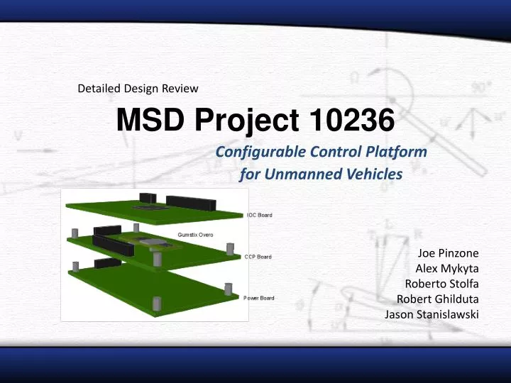
System Overview Power, Control Code Processor, I/O Controller are physically: • separable • stacked • enclosed
System Overview Power, IOC, CCP = Vehicle Controller Platform, separate from IOB
Power *All values are worst case
Power *All values are worst case
TPS43000-Based SW-MODE PSU OUTPUT 5V/1.5A 5V/0.25A IOB, ADC, DAC 4V/0.5A CCP 3.3V/0.5A IOC Battery Pack 2.5V/0.1A 1.2V/0.1A Power
Power • FRONT END CONDITIONING • TEXAS INSTRUMENTS TPS43000 • SEPIC (buck/boost) configuration • 1.8 – 9V Input • 6A output with proper FET switches • Synchronous Rectification (+eff)
Power • SECONDARY STAGELINEAR REGULATORS • LM317 ADJ. LDO • Low-drop-out • Vout 1.25 –> 5+ volts • Use for 5V, 4V • Up to 1.5A output • TLV70012 for 1.2V/200mA • TLV70025 for 2.5V/200mA • TPS73733 for 3.3V/0.50A
Nomenclature Firmware: • Program code that runs on the embedded processors. This does not include the Control Code, which will always be referred to specifically. Rigidware: • The HDL containing the “image” of the FPGA gate configuration. This may contain RAM/ROM initialization images and basic boot loader to initialize and load the stored firmware. This term generally pertains only to the IOC, since it is the only programmable-logic device in the system. Software: • Any program that runs on the user PC for the purpose of programming, configuring, compiling, or monitoring the embedded system.
IO Controller Module • Arbitrates IO from the CCP • Physically separable from CCP • Can be used as independent data logger or used in future projects. • Implemented using a Xilinx Spartan 3E FPGA (XCS500E-PQ208)
FPGA Selection • FPGA chosen for highest gate & largest pin count • BGA is not desirable due to board routing complexity
Main RAM • XC3S500E has 45KB of Block Memory • Approximately 40 KB will be used for Plasma CPU • RAM preloaded with boot loader
SPI FLASH & MMC • Application code is stored on SPI Flash • Boot loader loads application into RAM • Same SPI bus is used for an SD card for logging • All typical SD cards support standard MMC protocol
System Clock Counter • Provides timing information • Sourced from 50 MHz clock which allows for integer division to decade increments of time.
Dedicated UART • Hardwired to USB-UART transceiver • Load new application code • Debug system during operation
CCP Communication • Dual port ram allows for independent operation • High speed serial interface used to access shared RAM • Interrupt signals provided to and from CCP
Analog Controller • Finite state machine responsible for acquiring analog data from ADC • Data available for direct access from CPU address space • Configures reference voltage DAC
PWM Controller • FSM that arbitrates servo PWM generation and reading • Generator is configurable to provide servo format or full range duty cycles
Configurable IO Ports • Each pin can be configured as input, output, or special function • Special functions include configurable SPI, I2C and UART modules • IP provided by OpenCores
Configurable IO Ports • MAV peripheral set only requires 1 port • Preliminary logic estimates show that 5 ports should be possible
Programming Interface • USBUART converter does most of the work for us • PM FLASH is programmed from UART • Second UART is provided for CCP configuration
FLASH & SD Card • SST’s 4MB FLASH stores application program • Shares SPI Bus with SD Card for data logging and removable storage
CCP Interface • High speed serial interface to CCP along with interrupt requests • Pins on FPGA and header are reserved specifically for implementing GPMC in the future
FPGA Configuration • On power-up, FPGA is automatically configured by the XCF02S which stores rigidware. • Rigidware can be changed via JTAG interface
Analog to Digital Converter • Simultaneous samples of 8 channels • Supports differential inputs • Adjustable sampling range • Range is digitally controlled by adjacent DAC
Digital IO • PWM signals connected directly to IOB (3.3v levels) • Configurable IO Ports have adjustable logic levels. • User supplies voltage reference • TXB0108 detects direction of communication without the need for direction control
Logic Cost Analysis • Design with 5 IO ports uses approximately 80% of available logic • 20% for uncertainty in estimates and potential overhead for PAR of large designs.
Throughput Estimation • Dummy DAQ program written for MAV set of peripherals • Single sample can be executed in ~420 clock cycles @ 25 MHz • Assuming SPI communication to IMU is done without interrupts, CPU must stall for duration of transfer (~200 cycles @ 2 MHz) • Results in theoretical sample rate of 30 kHz
TI ADS1178 V- Calculation Airspeed Sensor: (4.7V + .2V)/2 = 2.45V Altitude Sensor: ( 4.5V + .5V)/2 = 2.5V Temperature Sensor: (4.986V + .229V) / 2 = 2.493V I/O Breakout Board Vref Calculation Airspeed Sensor: (4.7V - .2V)/2 = 2.25V Altitude Sensor: ( 4.5V - .5V)/2 = 2.0V Temperature Sensor: (4.986V -.229V) / 2 = 2.38V
Digital Peripherals: Tyco Electronics GPS – UART (NMEA) Analog Devices IMU – SPI Telemetry (P10231) – I2C, SPI, UART I/O Breakout Board
MUX IC Manual Override: 2 – Quad 2 to 1 multiplexers I/O Breakout Board
Molex 24 position connector Pitot-Static Probe (Airspeed) I/O Breakout Board Ram Air Pressure Stagnation (Static) Standard DSUB Connectors
CCP Overview • OMAP • ARM • Linux • Fixed point TI DSP • DSP/BIOS • running RT workshop Control System • Sensor data is memory mapped with DMA from the IO controller over a dedicated link
Incremental Design • Gumstix (target for MSD 2) • Ready-to-run system on a module • Self-sustained (low to no dependency count) • Readily available, non-existent lead time • Topedo SOM • Smaller + lower power consumption than Gumstix • Higher throughput achievable • Custom Board • Cheapest, fastest, most efficient yet most complicated solution • An implementation meeting every need marked “HIGH” has to be met before proceeding
Gumstix • Board requires nothing power • 2 expansion slots breakout McBSP and GPMC • Board lacks DMA support for GPMC • Implementation will use DMA with McBSP • DMA will be configured to routinely read data from McBSP and copy to a location in memory without interrupts • Slower than GPMC, uses less pins • Interface is well known • Target development time: 4 weeks
Torpedo • Second revision • Motivations: smaller board, GPMC with DMA becomes possible • Uses OMAP3530 (just as the Gumstix) • Product comes with verified schematics and layouts • Release date - late December • Expected price - $150 • Target development time: 4 weeks
Custom board • Reasons to improve on Torpedo • OMAP3525 is cheaper than the 3530 • TPS65920 consumes less power, requires less layout area (fewer discrete components are required) • Development time • Software and interface overlaps with Torpedo • Schematics and layout can mostly be reused
McBSP cont’d • Multi-channel Buffered Serial Port • (High speed serial) • Asynchronous Synchronous supported • DMA would be used to limit the use of the ARM processor • Maximum clock speed (bit speed) can use L4 clock (96MHz) • FPGA may not be able to reach this • Bit speed may need to be halved and channel count double