Download
1 / 26
260 likes | 350 Views
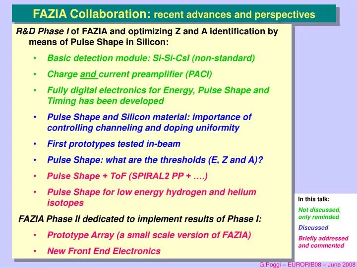
FAZIA Collaboration : recent advances and perspectives. R&D Phase I of FAZIA and optimizing Z and A identification by means of Pulse Shape in Silicon: Basic detection module: Si-Si-CsI (non-standard) Charge and current preamplifier (PACI)

E N D
FAZIA Collaboration: recent advances and perspectives • R&D Phase I of FAZIA and optimizing Z and A identification by means of Pulse Shape in Silicon: • Basic detection module: Si-Si-CsI (non-standard) • Charge and current preamplifier (PACI) • Fully digital electronics for Energy, Pulse Shape and Timing has been developed • Pulse Shape and Silicon material: importance of controlling channeling and doping uniformity • First prototypes tested in-beam • Pulse Shape: what are the thresholds (E, Z and A)? • Pulse Shape + ToF (SPIRAL2 PP + ….) • Pulse Shape for low energy hydrogen and helium isotopes • FAZIA Phase II dedicated to implement results of Phase I: • Prototype Array (a small scale version of FAZIA) • New Front End Electronics In this talk: Not discussed, only reminded Discussed Briefly addressed and commented G.Poggi – EURORIB08 – June 2008
ΔE1 ΔE2 Si Si CsI(Tl) H.I. ? 300μm 500 / 700μm 30-100 mm The FAZIA Initiative The FAZIA (Four Pi Z and A Identification Array) initiative was formalized in 2006. Members are from France, Italy, Poland, Spain, Rumania (+Canada, India and US). The goal of the present Phase I: studying and testing new solutions, checking if possible to make a step forward toward the “ideal” detector array for Dynamics and Thermodynamics of heavy-ion collisions at Fermi energies and below http://fazia.in2p3.fr • FAZIA PHASE I: Working Groups • Modeling current signals and Pulse Shape Analysis in Silicon (L.Bardelli) • Physics cases (G.Verde) • Front End Electronics (P.Edelbruck) • Acquisition (A.Ordine) • CsI(Tl) crystals (M.Parlog) • Single Chip Telescope (G.P.) • Design, Detector, Integration and Calibration (M.Bruno) • Web site (O.Lopez) G.Poggi – EURORIB08 – June 2008
O N C B Beyond E-E: Z and A Identification with Pulse Shape • Why Pulse Shape inSilicon is possible? • Stopped particles with the same energy and different Z (and A) show charge/current signals having unlike time evolution because ranges and plasma erosion times differ • Better identification for reverse-mount Silicon Energy vs rise-time of charge signals permits good Z identification of stopped particles (further identification criteria under study) A threshold exists for Z identification, for small particle penetration (a few tens of μm) Evidences exist that isotope separation (A identification) is possible above a certain penetration. First fully digital implementation of PSA in Silicon:L.Bardelli et al: NP A746 (2004) 272 G.Poggi – EURORIB08 – June 2008
82Se @ 408 MeV Elastic scattering on Au ~100 mm2 Silicon Current [a.u] ns Channeling and doping non -uniformity in Si for PSA Only very small scale implementation of high-quality PSA are reported in the literature (see Mutterer et al IEEE TNS 47 (2000) 756 ) G.Poggi – EURORIB08 – June 2008
82Se @ 408 MeV Elastic scattering on Au Current [a.u] ns Channeling and doping non -uniformity in Si for PSA Only very small scale implementation of high-quality PSA are reported in the literature (see Mutterer et al IEEE TNS 47 (2000) 756 ) Early FAZIA tests of our DPSA in Silicon with mono-energetic heavy-ions showed fluctuations in current and charge signal shape (also somewhat irreproducible) Basing on an older work (G.P. et al. NIM B119 (1996) 375) on channeling effects on stopped h.i.,we suspected that channeling (and Silicon doping non-uniformity) was originating these instabilities. Could this also explain overall irreproducibility of PSA quality observed in the past? The key experiment: collimated Silicon detectors mounted on a remote-controlled precision goniometer. Signal behavior as a function of the impinging ion direction with respect to crystal axes. Both <100> and <111> silicon detectors have been studied G.Poggi – EURORIB08 – June 2008
“Channeled” 80Se @ 408 MeV “Channeled” ns Signal Risetime and Channeling in <100> and <111> Silicon Our findings for “Channeled” or “random-entering” stopped ions Channeled ions: strongly fluctuating rise-time due to… enhanced variations of range and plasma erosion time for directions close to crystal channels, which are basically… G.Poggi – EURORIB08 – June 2008
“Random” 80Se @ 408 MeV 80Se @ 408 MeV “Channeled” “Random” Risetime-fluctuations vs gonio-angles ns ns Fluctuation increases <111> Si Signal Risetime and Channeling in <100> and <111> Silicon Our findings for “Channeled” or “random-entering” stopped ions Channeled ions: strongly fluctuating rise-time due to… enhanced variations of range and plasma erosion time for directions close to crystal channels, which are basically… … absent for random directions L.Bardelli et al; submitted to NIMA For <111> Silicon: typically 7° off-axis If detectors subtend ~1° and are mounted in theusual way, most ions may experience abnormal fluctuations, given the large channeling probability (ψ½ = 0.5°-1°) Channeling in Silicon is observed for front and rear injection G.Poggi – EURORIB08 – June 2008
80Se @ 408 MeV <100> Silicon “Channeled” “Random” Current [a.u] ns ns Signal Risetime and Channeling in <100> and <111> Silicon The mandatory recipe for good Pulse Shape Analysis: USE PURPOSELY ORIENTED SILICON DETECTORS for ALWAYS MAINTAINING RANDOM INCIDENCE! We have ordered indeed special-cut nTD wafers Irreproducibility: minor geometry variations of the setup change the fraction of channeled ions Unfortunately this does not explain everything… The Silicon doping uniformity must also be controlled up to an unprecedented level This information is basically not available from (detector/wafer)manufacturers L.Bardelli et al: submitted to NIMA G.Poggi – EURORIB08 – June 2008
R Fixed impact point Various bias voltage Over depletion Full bias Slightly under-bias T_rise Resistivity measurements (doping uniformity) in Silicon A newly developed procedure to map Silicon resistivity, based on Transient Current Technique has been systematically applied to our detectors Narrow UV laser pulse (ns) Si detector Reverse-mount Silicon det. Various applied voltages: from under- to over bias G.Poggi – EURORIB08 – June 2008
R Fixed impact point Various bias voltage Over depletion Full bias Slightly under-bias T_rise Resistivity measurements (doping uniformity) in Silicon A newly developed procedure to map Silicon resistivity, based on Transient Current Technique has been systematically applied to our detectors A typical detector: ~9% non-uniformitywith striations (mm-1 spatial frequency) Narrow UV laser pulse (ns) Si detector Reverse-mount Silicon det. Various applied voltages: from under- to over bias G.Poggi – EURORIB08 – June 2008
R Fixed impact point Various bias voltage Over depletion Full bias Slightly under-bias T_rise Resistivity measurements (doping uniformity) in Silicon A newly developed procedure to map Silicon resistivity, based on Transient Current Technique has been systematically applied to our detectors Narrow UV laser pulse (ns) Si detector A non typical, very good detector: ~1% non-uniformitywith undetectable striations Memento: good resistivity uniformity good uniformity of electric field position independence of timing Reverse-mount Silicon det. Various applied voltages: from under- to over bias G.Poggi – EURORIB08 – June 2008
Quasi-random entering ions Channeled ions Random entering ions Wrong detector mounting causes some residual planar channeling PSA test run with full control of channeling and resistivity 32S + 27Al @ 474 MeV(LNL, December 2007) Si-Si, Si-CsI and “Single Chip Tel” have been used. All Silicons were characterized for uniformity, were un-collimated and have the “FAZIA” dimensions(400mm2) PACI preamps A fully digital FEE for charge and current PSA has been developed (Orsay+Florence) for Phase I Channeling control for the experiment: Detectors made of random-cut Silicon were not yet available All detectors are cut 0° off <111> axis Channeling--random control obtained by proper 7° detector tilting (simple mechanical adjustment permits to switch from unwanted channeling to desired “random” orientations) G.Poggi – EURORIB08 – June 2008
32S + 27Al @ 474 MeV (December 2007) Channelor not to channel? DIGITAL PULSE SHAPE on 500μ Silicon Full scale: ~1.5 GeV 32S +27Al @ 474 MeV Normally impingingions Are channeling effects really important? F Pulser Ne O Na 300 μ 500 μ N Very uniform500μm Silicon Standard mounting, i.e. perpendicular ion incidence is expected to induce channeling Satisfactory Z identification over the full examined range C B Be G.Poggi – EURORIB08 – June 2008
32S + 27Al @ 474 MeV (December 2007) Channel ornot to channel? DIGITAL PULSE SHAPE on 500μ Silicon Full scale: ~1.5 GeV 32S +27Al @ 474 MeV Yes, they are! Channeling was spoiling mass identification Randomimpingingions F Pulser Ne O Na 300 μ 500 μ N Very uniform500μm Silicon Channeling was partly spoiling overall identification Random:7° tilt angle Mass identification clearly shows up! C B Be G.Poggi – EURORIB08 – June 2008
32S + 27Al @ 474 MeV (December 2007) Channelor not to channel? DIGITAL PULSE SHAPE on 500μ Silicon Full scale: ~ 4 GeV 32S +27Al @ 474 MeV S Normallyimpingingions Cl P Ar Si K Al Mg 500 μ Na Ne F Very uniform500μm Silicon Standard mounting, i.e. perpendicular ion incidence Satisfactory Z identification over the full examined range Note the very high energy range O N C B Be Unity counts removed G.Poggi – EURORIB08 – June 2008
32S + 27Al @ 474 MeV (December 2007) Channel or not to channel? DIGITAL PULSE SHAPE on 500μ Silicon Full scale: ~ 4 GeV 32S +27Al @ 474 MeV S Random impingingions Cl P Ar Si K Al Mg 500 μ Na Ne F Very uniform500μm Silicon Channeling was partly spoiling identification “Random”mounting O N C B Be Unity counts removed G.Poggi – EURORIB08 – June 2008
140V on 300μm 9.4% non-uniformity S P Cl? Si Ar? Al Mg Na Ne F O N C 300 μ B Be 250V on 500μm 1% non-uniformity S Cl Ar P Si K Al Ca Mg Na Ne F O N C 500 μ B Be 32S + 27Al @ 474 MeV (December 2007): doping uniformity DIGITAL PULSE SHAPE on 500μm and 300μm Silicons with similar field and different doping non-uniformities 300μm: ~ 4 GeV full scale 500μm: ~ 4 GeV full scale Quasi-random, but non-uniform Silicon shows reasonable Z resolution Quasi-random,very uniformSilicon shows clean Z and partial A resolution G.Poggi – EURORIB08 – June 2008
Al 140V on 300μm 9.4% non-uniformity Mg Na S P Ne Cl? Si Ar? Al F Mg Na O Ne F O N N C B Be 140V on 300μm 9.4% non-uniformity C Al Mg 250V on 500μm 1% non-uniformity Na Ne S Cl Ar P Si K F Al Ca Mg Na O Ne F O N N C 500 μ B C Be 250V on 500μm 1% non-uniformity 32S + 27Al @ 474 MeV (December 2007): doping uniformity DIGITAL PULSE SHAPE on 500μm and 300μm Silicons with similar field and different doping non-uniformities 300μm: ~ 4 GeV full scale 500μm: ~ 4 GeV full scale Quasi-random, but non-uniform Silicon shows reasonable Z resolution 300 μ Quasi-random,very uniformSilicon shows clean Z and partial A resolution 500 μ G.Poggi – EURORIB08 – June 2008
60Ni 58Ni FAZIA Phase I: Digital Pulse Shape on Silicon Preliminary conclusions: with uniformity-controlled and “random”-oriented Silicon detectors, Digital PSA developed in FAZIA permits unity charge resolution at least up to Z ~ 30 (probably >50), with energy thresholds of about 3MeV/n for C and 4MeV/n for Ne (about 30-40 μm of Silicon) DPSA gives mass resolution for Z<15-20(also based on short-run results with 58,60Ni) particles, with ranges > 100μm (?) of Silicon ToF might significantly extend this mass resolution Frankly, we are not unhappy about these preliminary results… G.Poggi – EURORIB08 – June 2008
3rd vs 2nd moment of current signals Exp+Sim Y axis: measured energy X axis: measured rise-time + simulated ToF over 1.1m and 0.5 ns FWHM (smoothly merged) FAZIA Phase I: next steps Best algorithms for DPSA are under study within FAZIA WG1 (S.Barlini et al: in preparation) Adding ToF to current or charge risetime for extending mass resolution of low energy stopped particles Trying to get ToF even with non-optimal time structure of the pulsed beam (supported by Spiral2 PP) Addressing Digital Pulse Shape for Silicon strip and Z = 1,2 ions (supported by Spiral2 PP) Future experiments: LNL, LNS, GANIL… G.Poggi – EURORIB08 – June 2008
~104 telescopes x 8 FAZIA R&D Phase II (and Phase III) • Phase II (from 2008 till 2012): • Prototype Array (20-30 modules) to couple with existing arrays and do Physics out of it • Implement the solutions devised and tested on Phase I • adopt electronic and mechanical solutions as close as possible to the final 4π configuration (e.g. neutron detection feasibility and transportability) • Phase III (from 2012 on): • Build a Demonstrator, covering a significant fraction of 4π, e.g C2+C1 C2 C1 C3 C4 A possible final FAZIA Array (JM Gautier-LPC) G.Poggi – EURORIB08 – June 2008
Data transmission to PC farm Trigger decision (400 ns) Trigger validation and event labeling Trigger Box DAQ Ethernet Trigger info ..64.. Samples Trigger and data collector + dispatcher Trigger/samples separation and trigger elaboration Trigger info and samples 2.2 Gb/s Trigger validation and slow control 2.2 Gb/s Air Vacuum Fast and slow Energy shaping Local digital trigger generation (100 ns)+ second level decision (over in 2-3 μs)+ data sending (asynchronous) First Level FEE Unit First Level FEE Unit First Level FEE Unit ..16.. ..16.. ..16.. ..640.. FAZIA R&D Phase II: the FEE FEE structure under vacuum to simplify connections (the very issue under study: power removal) Bidirectional fast (2.2 Gb/s) fiber optics guaranteessynchronous trigger infotransmission and transfer of samples (data). The last level provides trigger construction / validation / event labeling + sample dispatching to DAQ Fast FPGA-based elaboration and protocol management G.Poggi – EURORIB08 – June 2008
The FAZIA organization • FAZIA Working Groups • Modeling current signals and Pulse Shape Analysis (L.Bardelli) • Physics cases (G.Verde) • Front End Electronics (P.Edelbruck) • Acquisition (A.Ordine) • CsI(Tl) crystals (M.Parlog) • Single Chip Telescope (G.P.) • Design, Detector, Integration and Calibration (M.Bruno) • Web site (O.Lopez) FAZIA Project Management Board:B.Borderie, R. Borcea, R.Bougault, A.Chbihi, F.Gramegna, T.Kozik, I.Martel Bravo, E.Rosato, G.P. and R.Roy Sc. Coordinators: G.P. and R.Bougault Tech. Coordinator: P.Edelbruck A dedicated Discussion Group is studying the Physics requirements for the Trigger (M.F.Rivet and A.Olmi) to implement with our electronic engineers Two more slides on “synergies” G.Poggi – EURORIB08 – June 2008
Elastic scattering in 93Nb+116Sn @ 30 MeV/n E E Synergies in instrumentation Questions fitting very well with our Topic Is channeling an issue only for PSA-based identification? How about channeling and more standard identification approaches? Significant effects are expected in E-E: channeling may change E, as many of us have seen when punching-through elastic scattering is measured This effect is less clearly appreciated in other cases, but still present G.Poggi – EURORIB08 – June 2008
300 μ 500 μ 32S + 27Al @ 474 MeV (December 2007) Digital E-E 300-500μ Silicon (reverse field) Full scale E: ~4GeV Full scale E: ~1.5 GeV 32S +27Al @ 474 MeV Try a little, proper detector tilting … Na Ne Normallyimpinging ions F O N C B Telescope mountedfor standard normal incidence Why so-so resolution? Never happened to you? Be Li Unity counts removed G.Poggi – EURORIB08 – June 2008
300 μ 500 μ 32S + 27Al @ 474 MeV (December 2007) Beneficial effects of random incidence for standard E-E identification Digital E-E 300-500μ Silicon (reverse mount) Full scale E: ~4GeV Full scale E: ~1.5 GeV 32S +27Al @ 474 MeV … say channeling “goodbye” Na Ne Randomimpinging ions F We believe that one should keep this result in mind for any future E(Si)-Eimplementation. Do not overlook the old recommendation of 7° off-axis cutand double check what you buy. Thanks to the audience O N C B Telescope mounted for 7° incidence(Quasi-randomconfiguration) Be Li Unity counts removed G.Poggi – EURORIB08 – June 2008