Semiconductor Fundamentals: Band Structures and Doping Mechanisms Explained
220 likes | 247 Views
This lecture outlines essential semiconductor quantities, energy band models, band gap energy, density of states, and doping mechanisms in the context of Silicon crystal structures. Learn about donors, acceptors, and charge carrier concentrations.

Semiconductor Fundamentals: Band Structures and Doping Mechanisms Explained
E N D
Presentation Transcript
Lecture 2 OUTLINE • Important quantities • Semiconductor Fundamentals (cont’d) • Energy band model • Band gap energy • Density of states • Doping Reading: Pierret 2.2-2.3, 3.1.5; Hu 1.3-1.4,1.6, 2.4
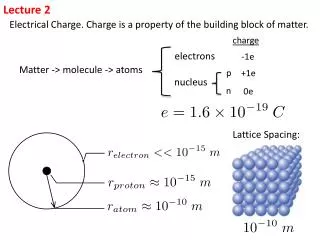
Important Quantities • Electronic charge, q = 1.610-19 C • Permittivity of free space, eo = 8.85410-14 F/cm • Boltzmann constant, k = 8.6210-5 eV/K • Planck constant, h = 4.1410-15 eVs • Free electron mass, mo = 9.110-31 kg • Thermal voltage kT/q = 26 mV at room temperature • kT = 0.026 eV = 26 meV at room temperature • kTln(10)= 60 meV at room temperature 1 eV = 1.6 x 10⁻¹⁹ Joules EE130/230M Spring 2013 Lecture 2, Slide 2
Si: From Atom to Crystal Energy states in Si atom energy bands in Si crystal • The highest nearly-filled band is the valence band • The lowest nearly-empty band is the conduction band EE130/230M Spring 2013 Lecture 2, Slide 3
Energy Band Diagram • Simplified version of energy band model, showing only the bottom edge of the conduction band (Ec) and the top edge of the valence band (Ev) • Ec and Ev are separated by the band gap energy EG Ec electron energy Ev distance EE130/230M Spring 2013 Lecture 2, Slide 4
Electrons and Holes (Band Model) • Conduction electron = occupied state in the conduction band • Hole = empty state in the valence band • Electrons &holes tend to seek lowest-energy positions Electrons tend to fall and holes tend to float up (like bubbles in water) electron kinetic energy Ec represents the electron potential energy. Ec Increasing electron energy Increasing hole energy Ev hole kinetic energy EE130/230M Spring 2013 Lecture 2, Slide 5
Electrostatic Potential, Vand Electric Field, E • The potential energy of a particle with charge -q is related to the electrostatic potential V(x): • Variation of Ec with position is called “band bending.” 0.7 eV EE130/230M Spring 2013 Lecture 2, Slide 6
Measuring the Band Gap Energy • EG can be determined from the minimum energy of photons that are absorbed by the semiconductor Ec photon hn > EG Ev Band gap energies of selected semiconductors EE130/230M Spring 2013 Lecture 2, Slide 7
Density of States E dE Ec Ec density of states, g(E) Ev Ev g(E)dE = number of states per cm3 in the energy range between E and E+dE Near the band edges: Electron and hole density-of-states effective masses for E Ec for EEv EE130/230M Spring 2013 Lecture 2, Slide 8
EG and Material Classification silicon dioxide silicon metal • Neither filled bands nor empty bands allow current flow • Insulators have large EG • Semiconductors have small EG • Metals have no band gap (conduction band is partially filled) Ec Ec Ev EG = 1.12 eV EG = ~ 9 eV Ev Ec Ev EE130/230M Spring 2013 Lecture 2, Slide 9
Donors: P, As, Sb Acceptors: B, Al, Ga, In Doping • By substituting a Si atom with a special impurity atom (Column V or Column III element), a conduction electron or hole is created. ND ≡ ionized donor concentration (cm-3) NA ≡ ionized acceptor concentration (cm-3) EE130/230M Spring 2013 Lecture 2, Slide 10
Doping Silicon with a Donor Example: Add arsenic (As) atom to the Si crystal The loosely bound 5th valence electron of the As atom “breaks free” and becomes a mobile electron for current conduction. EE130/230M Spring 2013 Lecture 2, Slide 11
Doping Silicon with an Acceptor Example: Add boron (B) atom to the Si crystal The B atom accepts an electron from a neighboring Si atom, resulting in a missing bonding electron, or “hole”. The hole is free to roam around the Si lattice, carrying current as a positive charge. EE130/230M Spring 2013 Lecture 2, Slide 12
Doping (Band Model) Donor ionization energy Ec ED EA Ev Acceptor ionization energy Ionization energy of selected donors and acceptors in silicon EE130/230M Spring 2013 Lecture 2, Slide 13
Dopant Ionization EE130/230M Spring 2013 Lecture 2, Slide 14
Charge-Carrier Concentrations Charge neutrality condition: ND + p = NA + n At thermal equilibrium, np = ni2 (“Law of Mass Action”) Note: Carrier concentrations depend on net dopant concentration! EE130/230M Spring 2013 Lecture 2, Slide 15
n-type Material (n > p) ND > NA(more specifically, ND – NA >> ni): EE130/230M Spring 2013 Lecture 2, Slide 16
p-type Material (p > n) NA > ND(more specifically, NA – ND >> ni): EE130/230M Spring 2013 Lecture 2, Slide 17
Carrier Concentration vs. Temperature EE130/230M Spring 2013 Lecture 2, Slide 18
Terminology donor: impurity atom that increases n acceptor: impurity atom that increases p n-type material: contains more electrons than holes p-type material: contains more holes than electrons majority carrier: the most abundant carrier minority carrier: the least abundant carrier intrinsic semiconductor: n = p = ni extrinsic semiconductor: doped semiconductor such that majority carrier concentration = net dopant concentration EE130/230M Spring 2013 Lecture 2, Slide 19
Summary • Allowed electron energy levels in an atom give rise to bands of allowed electron energy levels in a crystal. • The valence band is the highest nearly-filled band. • The conduction band is the lowest nearly-empty band. • The band gap energy is the energy required to free an electron from a covalent bond. • EG for Si at 300 K = 1.12 eV • Insulators have large EG; semiconductors have small EG EE130/230M Spring 2013 Lecture 2, Slide 20
Summary (cont’d) • Ec represents the electron potential energy Variation in Ec(x) variation in electric potential V Electric field • E - Ec represents the electron kinetic energy EE130/230M Spring 2013 Lecture 2, Slide 21
Summary (cont’d) • Dopants in silicon: • Reside on lattice sites (substituting for Si) • Have relatively low ionization energies (<50 meV) ionized at room temperature • Group-V elements contribute conduction electrons, and are called donors • Group-III elements contribute holes, and are called acceptors Dopant concentrations typically range from 1015 cm-3 to 1020 cm-3 EE130/230M Spring 2013 Lecture 2, Slide 22