Download
1 / 24
240 likes | 374 Views
LLRF Developments at the BNL Collider-Accelerator Department. K. S. Smith (for the C-AD RF Group). People Involved in the C-AD LLRF Upgrade Effort. Group Leader Emeritus J. M. Brennan (Stochastic Cooling) Group Leader A. Zaltsman Deputy Group Leader T. Hayes

E N D
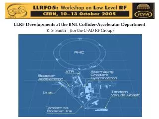
LLRF Developments at the BNL Collider-Accelerator Department K. S. Smith (for the C-AD RF Group)
People Involved in the C-AD LLRF Upgrade Effort Group Leader Emeritus J. M. Brennan (Stochastic Cooling) Group Leader A. Zaltsman Deputy Group Leader T. Hayes RF Accelerator Physicist M. Blaskiewicz (Stochastic Cooling) Controls Engineering L. Hoff (C-AD Controls Group) LLRF Engineer J. DeLong LLRF / HLRF / Controls Engineer F. Severino LLRF Engineer K. S. Smith Operations Liaison K. Zeno (C-AD Operation Group)
Motivation for Upgrading the C-AD LLRF Systems • RHIC LLRF System • The heart of the RHIC LLRF, a COTs quad TI-C40 DSP VME module (LSI / Spectrum) , is ~ 10 years old, obsolete and we have only 1 ½ spare. • RHIC RF operating modes have evolved over the 6 years since RHIC commissioning began. • AGS and Booster LLRF Systems • Rely on a hybrid system of older analog modules and newer VME based digital hardware (AGS/Booster Upgrade, SNS Ring LLRF). • Completely different hardware than RHIC LLRF. • Spares issues. New operational needs. • LLRF Systems for new projects • SC Energy Recovery LINAC and 1MW SC Photocathode Gun • Our first foray into SCRF and energy recovery • Electron Beam Ion Source • New heavy ion injector for Booster (RHIC)
Factors Influencing the Architecture Decision • We don’t have the manpower or the time to develop custom application specific solutions for each LLRF system. • RHIC needs upgrade yesterday. • AGS and Booster need upgrade now. • New projects need new LLRF systems soon. • Current operating schedule is very busy. • We have only four LLRF engineers for all of this. • We don’t want a custom solution for each system anyway. • The existing differences between RHIC, AGS and Booster LLRF already make operation, maintenance and development difficult enough. • We don’t have the manpower to assign specific experts to operate, maintain and develop each system. Everyone must know every system.
The Solution • Design a generic, modular LLRF control architecture which can be configured to satisfy all of the LLRF control demands we currently have, and which will be supportable and upgradeable into the foreseeable future. • Architecture has evolved from design and operational experiences with digital LLRF control hardware for RHIC, and more recent experience with the AGS, Booster, and SNS Ring LLRF design efforts. • Two major components: • System Carrier Board • Self supporting (stand alone) LLRF system controller and control system interface. • Custom Daughter Modules • Provide system specific data acquisition capability and processing horsepower. • DSP, ADC, DAC, etc. • Obviously other support modules around this (primarily NIM analog). • Huge engineering challenge, but the potential benefits justify it.
Potential Benefits • Designing a common modular architecture for all systems: • minimizes the number of new components we need to design, and allows us to focus limited engineering resources most effectively. • maximizes the potential for re-use of both hardware and firmware. • eases the operational burden. • common hardware and user interfaces across all systems. • eases maintenance issues. • common hardware across all systems is more easily serviced; ready spares are easier to maintain. • eases system development. • flexible, expandable, readily configurable and quickly deployable. • eases the control system support burden. • application development, software configuration, code modularity.
Big Learning Curve and Many Obstacles to Overcome • First production hardware ready in Oct 2007 (LLRF07 ?) using devices, software development tools, technologies, standards and protocols we have never used before: • Xilinx V4FX60-1152 FPGA • Incredible amount of documentation to pour over (5000+ pages) • Entirely new FPGA hardware architecture for us (coming from Altera) • Entirely new development environment for us • ISE Foundation • EDK (Embedded Developers Kit) • Platform Studio • Must standardize on and become proficient in VHDL • PCI bus protocol and hardware implementation, in FPGA and on PCB • Xilinx MGTs (Multi Gigabit Transceivers) • Xilinx Aurora Channel Protocol (lightweight serial communication protocol) • Ethernet into our hardware for first time • DDR SDRAM interfacing • TigerSHARC DSP hardware architecture and development environment • New PCB design and layout challenges
Xilinx V4FX60 - 1152 • We have standardized on one FPGA for all system components. Big part of previously mentioned big learning curve, but then we leverage off design re-use across systems. • 1.2V core voltage • Dual Embedded Power PC 405 hard cores @ 450 MHz • 4 embedded Ethernet MACs • 16 Multi-Gigabit Transceivers (MGTs) • Full duplex serial transceivers up to 10 Gb/s. • 128 cascadeable 500 MHz 18 x 18 signed multiply / accumulate • Signal processing horsepower • Global / Regional Clocks, Digital Clock Managers (DCMs), Phase Matched Clock Dividers (PMCDs) • 232 18 kb memory blocks @ 500 MHz (4 Mb) • 576 User IO pins • SelectIO, DCI, per bit de-skew, integrated serdes (1 Gb/s)
System Carrier Board Major Subcomponents • Xilinx V4FX60 • Stand alone LLRF system controller and control system interface. • The C-AD Controls System is standardized around VME, with MVME-2100 PowerPC FECs (Front End Computers, like EPICS IOCs) running VxWorks. • The PPC405 allows us to embed this functionality directly into our own hardware. MVME-2100 and VME not necessary. • Allows us to leverage the full spectrum of (existing) C-AD Controls software, and radically eases development efforts for any new software. • L. Hoff has already ported C-AD Controls software to evaluation board. • PowerPC to PCI bridge and generic PCI interface IP enables us to use PCI as the local bus on the carrier. • Allows us to standardize on PMC as the format for our daughter cards. • Convenient standard interface (mechanical and electrical) for us to use. • Permits use of COTs PMC modules (lots out there) if desired. • Primarily intended as a configuration bus.
System Carrier Board Major Subcomponents • Xilinx V4FX60 (cont.) • MGTs provide us with very high speed serial system interconnect. • Too difficult to route multiple high speed parallel buses (PCI is enough work). • A fast PTP system interconnect, chip to chip, box to box, machine to machine. • Can implement other protocols if desired. Just change the IP. • Can just use MGT as a very fast SERDES. • T. Hayes has successfully tested a Xilinx Aurora Channel at 2 Gb/s. • Lightweight, low latency, non-switched. Suitable for feedback loops. • Routes C-AD Control System broadcast data links from rear panel. • C-AD machine parameters and system timing are broadcast over several Controls System serial links (RTDL, Event, Beam Sync). • Routes external clocks and triggers from rear panel. • Interface to Modular SODIMM SDRAM and FLASH • Diagnostic data, configuration data, OS usage
System Carrier Board Major Subcomponents • CML / LVDS crosspoint allows flexible configuration of system interconnects. • AD8152, 3.2 Gb/s, 34 x 34 crosspoint switch • Allows maximum flexibility in the routing of gigabit serial links depending on system requirements. • Configurable high speed interconnects between Carrier V4FX60, Carrier rear panel signals, and daughter sites. • Could use V4FX60 as crosspoint if “one hop” latency is acceptable. • Power Regulation and Distribution • Many different power supply voltages which need to be produced and distributed. • PCI standard voltages (+3.3VD, +5VD, +/- 12V) • FPGA and DSP core (+1.2V) and IO (+3.3VD, +2.5VD) voltages. • Permits us to choose technology (switching, linear) to suit our performance needs. • RHIC Master Clock (and ERL) must be extremely low phase noise, low spurs. • Not only analog which needs “quiet” power. High speed serial links can be very fussy and susceptible to power supply noise (deterministic jitter). • Reduce as much as possible the need for regulators on daughter modules. • Reduce footprint and power dissipation on daughter modules.
System Carrier Board Major Subcomponents • PMC Daughter Sites • Supports minimum of four 33 MHz / 32 bit PMC daughter mezzanine sites • Number of sites only limited by PCI signaling specification. • PCI/PMC standard provides for +3.3V, +5V, and +/- 12V to daughter sites. • We pseudo-violate PMC spec w.r.t. the PMC P3 connector (64 bit extension). • Assign a number of P3 pins as jumper selectable power pins. • “Quiet” power from Carrier to Daughter Modules. • Daughters also have jumpers for compatibility with COTS carriers. • PMC P4 (“User Defined” a la VME P2 outer rows) • Six Aurora full duplex channels per daughter site @ up to 3 Gb/s each • Clock and trigger distribution • Spare IO • Controls System data and timing links (RTDL, Event, Beam Sync)
PMC Daughter Modules • All PMC daughter modules will make maximum re-use of common functionality. • After common functionality is debugged once, engineers focus only on custom aspects. • V4FX60 Standard Functionality re-used on daughters • Carrier interface • PCI interface • Standard PMC power via PMC P1 and P2 • “Quiet” power via PMC P3 • PMC “User Defined” P4 connections • Six full duplex Aurora channels at 3 Gb/s • Site specific clocks, triggers, and spare IO • Control System links (RTDL, Event, Beam Sync) • FPGA configuration device accessible from PCI • SODIMM DDR SDRAM interface, FLASH interface
PMC Daughter Modules • DSP Module • We are still firm proponents of DSP, including DSP in loops. • There are a lot more people who can code/read C than VHDL. • Late night on the fly re-coding of DSP firmware much easier than FPGAs. • Floating point math. • Ethernet to front panel, 4 Aurora channels to front panel • Quad DSP cluster based on ADSP-TS201 SABP-060, 576 pin BGA • 600 MHz core instruction rate, 7.5x our prior generation DSP (ADSP-21160) • Example Improvement: PID loop for cavity IQ control • ADSP-21160 executes in about 600ns • ADSP-TS201 executes in about 80ns before optimizing for TS201. • 24 Mb internal SRAM • 64 bit external bus with glueless interface for DSP clusters • 4 x 128 bit internal data / instruction buses • Up to four instructions issued per clock cycle • Dual fixed/floating point compute units operate SIMD or independent • 8 MACs per cycle peak (7.1 MACs per cycle sustained) 16-bit performance. • 2 MACs per cycle peak (1.8 MACs per cycle sustained) 32-bit performance. • 6 single-precision floating-point operations per cycle (3.6 GFLOPS). • 24 fixed-point (16-bit) operations per cycle (14.4 GOPS).
PMC Daughter Modules • ADC and DAC Modules • 8 channels per board with SMC or other front panel connectors • 2 clock, 4 GPIO, and 1 Aurora FD to “ready” connection on PCB. • ADC and DAC chips chosen for convenience for first pass hardware • ADC • AD9245 14 bit, 80 MSPS, 7 cycle pipeline, 0.5 DNL / 1.4 INL (LSB) • DAC • AD9754 14 bit, 125 MSPS, 0.75 DNL / 1.5 INL (LSB) • Both used for Booster/AGS and SNS Ring LLRF hardware (perform very well). • “State of the Art” surpasses this performance. Extremely interested in other’s experiences. • What issues to watch out for? • Pipeline delays adding too much latency? • PLLs or other clock conditioning? Some systems with large dF and Fdot. • DC accuracy and stability - need separate baseband ADC/DAC boards? • Sampling methods?
Diagnostic Data Acquisition • While we think we have significant diagnostic data storage and transfer capabilities designed into the system, we are only just beginning to think about how to manage this. • Acquisition modes • Routine logging mode • Post mortem w/ high resolution to determine cause and effect • Triggered (pre & post) • Low level hardware perspective vs. high level application • Alignment of timestamps between machines • DSP assumed to be the data source for system
Summary • See prior slides …
The End • End of Presentation