Download
1 / 1
10 likes | 113 Views
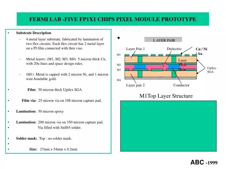
L AYER PAIR. Cu / Ni / Au. L. aye. r. P. a. ir. 1. D. i. e. l. ec. tri. c. Laser Thru-Hole. L. aye. r. pa. ir. 2. Condu. c. to. r. FERMI LAB -FIVE FP1X1 CHIPS PIXEL MODULE PROTOTYPE. Substrate Description

E N D
L AYER PAIR Cu / Ni / Au L aye r P a ir 1 D i e l ec tri c Laser Thru-Hole L aye r pa ir 2 Condu c to r FERMI LAB -FIVE FP1X1 CHIPS PIXEL MODULE PROTOTYPE • Substrate Description • 4 metal layer substrate, fabricated by lamination of two flex circuits. Each flex circuit has 2 metal layer on a PI film connected with thru vias. • Metal layers: (M1, M2, M3, M4) 5 micron thick Cu, with 20u lines and space design rules. • (M1) Metal is capped with 2 micron Ni, and 1 micron wire-bondable gold. • Film: 50 micron thick Upilex SGA • Film via: 25 micron via on 108 micron capture pad. • Lamination: 50 micron epoxy • Lamination: 200 micron via on 350 micron capture pad. • Via filled with SnSb5 solder. • Solder mask: Top - no solder mask. • Size: 27mm x 54mm x 0.2mm M1 M2 M3 M4 Upilex-SGA M1Top Layer Structure ABC-1999