Advanced 4-Metal Layer Substrate Prototype for High-Precision Electronics
10 likes | 127 Views
This document outlines the specifications of a prototype substrate designed for high-performance electronic applications. The substrate features a sophisticated 4-metal layer structure fabricated through the lamination of two flexible circuits, with each circuit comprising two metal layers. Key attributes include 5-micron thick copper layers (M1-M4), along with nickel capping and gold finish for optimal conductivity. The substrate is enhanced with 50-micron thick Upilex SGA film and utilizes advanced vias for connections. Ideal for applications requiring precision and reliability.

Advanced 4-Metal Layer Substrate Prototype for High-Precision Electronics
E N D
Presentation Transcript
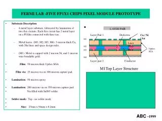
L AYER PAIR Cu / Ni / Au L aye r P a ir 1 D i e l ec tri c Laser Thru-Hole L aye r pa ir 2 Condu c to r FERMI LAB -FIVE FP1X1 CHIPS PIXEL MODULE PROTOTYPE • Substrate Description • 4 metal layer substrate, fabricated by lamination of two flex circuits. Each flex circuit has 2 metal layer on a PI film connected with thru vias. • Metal layers: (M1, M2, M3, M4) 5 micron thick Cu, with 20u lines and space design rules. • (M1) Metal is capped with 2 micron Ni, and 1 micron wire-bondable gold. • Film: 50 micron thick Upilex SGA • Film via: 25 micron via on 108 micron capture pad. • Lamination: 50 micron epoxy • Lamination: 200 micron via on 350 micron capture pad. • Via filled with SnSb5 solder. • Solder mask: Top - no solder mask. • Size: 27mm x 54mm x 0.2mm M1 M2 M3 M4 Upilex-SGA M1Top Layer Structure ABC-1999