Download
1 / 15
150 likes | 261 Views
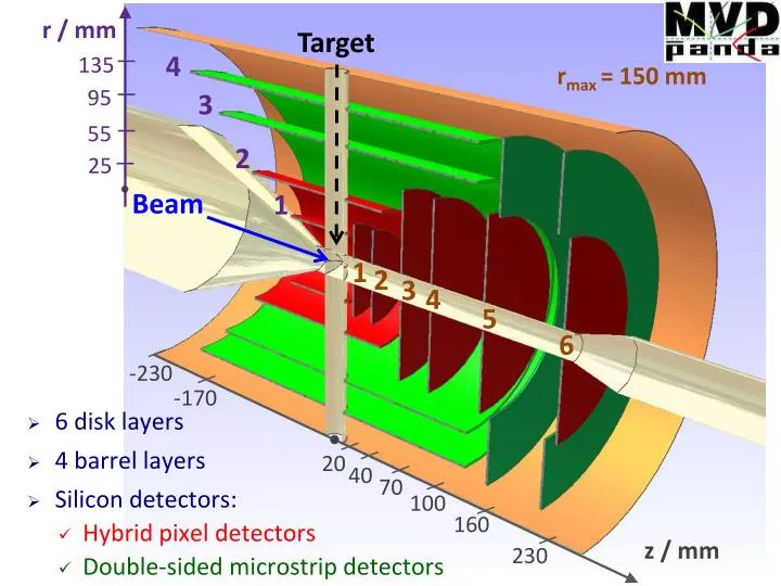
r / mm. Target. 4. r max = 150 mm. 3. 2. 135. 1. Beam. 95. 1. 55. 2. 3. 4. 25. 5. 6. -230. -170. 6 disk layers 4 barrel layers Silicon detectors : Hybrid pixel detectors Double - sided microstrip detectors. 20. 40. 70. 100. 160. 230. z / mm. Target. Beam.

E N D
r / mm Target 4 rmax= 150 mm 3 2 135 1 Beam 95 1 55 2 3 4 25 5 6 -230 -170 • 6 disk layers • 4 barrel layers • Silicon detectors: • Hybrid pixel detectors • Double-sided microstripdetectors 20 40 70 100 160 230 z / mm
Target Beam • Implementation • Approx. 11 million pixel readout channels • Approx. 200. 000strip readout channels
Detailed CAD model Detector simulation Detailed model including routing Active detector volumes only
Overall routing concept (7.6 … 15.0) cm Circular occupancy Bundling (top/bottom) Beam Circular or bundled Patch Panels 60 z / cm -100 -40 -23 0
Main MVD parts Overall detector integration 2 pixel half-barrels 2 strip half-barrels 6 pixel half-disks 2 strip half-disks MVD attachment Global frame (MVD): 2 halves 3 point fixation Central support frame
Mechanics • Cooling concept • Coolant: Water (18°C) • Vacuum-operated mode using hydrostatic pressure • Active part: ext 2 mm pipe (Ni-Co alloy) • Upstream routing: ext 4 mm flexible plastic pipes Barrel layer Infrared image Micro fittings: Thermoplastic resin 31°C 23°C Glue: Epo-Tek H70 Glue: Master Bond Glue: ArticSilver Thermal FEM analysis Tmax = 37.2°C Tmax = 28.2°C Tmax = 30.4°C Test setup
Mechanics • Lightweight support structures Local support (barrel modules) MVD half support frame R = 137 mm L = 460mm S = 3.8 mm • Sandwich structure: (Carbon – Rohacell – Carbon) • Stiffening structure:2...4 layers of carbon fibre (400 m) HTC foam half disk embedding cooling pipes Barrel layer support
Detector development: Front end electronics • ToPix: Custom designed readout chip • Specifications • Untriggered readout • High output bandwidth • 116 110 pixel matrix (100 100 m2 cell size) • Time over threshold technique (TOT) for amplitude measurement • Low power consumption (< 500 mW/cm2) • CMOS 130 nm technology • Measurements • Testing procedures • Total ionizing dose test • ToPix prototype connected to epi-sensor
Detector development • Pixel sensor • Specifications • Epi-Silicon layer: (50 ... 100) m • Thinned Cz silicon substrate: 50 m • Alt.: Thinned oxygen enriched silicon • Measurements • Sensor characterization • Radiation damage test (neutrons)
Count rates • Maximum countrates / frontend: (1 ... 10) Mevts/ s • Integrated count rate (pixel part): 1.8 Gevts / s • Integrated count rate (strip part): 1.2 Gevts / s Full MVD: 3.0 Gevts / s
Spatial coverage • 2D mapping: Number of MVD points / track • Design optimization for a minimum of 4 track points Active MVD volumes Number of MVD points / track
Radiation length studies (Geantino) • 1D profile scan for polar angle • Minimized material budget for polar angle < 140° • Higher values above 140° due to upstream routing • Slight enhancement 40° due to lead-out of pixel disk services Detailed MVD model < 1% / layer ( < 10%)
Momentum resolution 1 GeV/c pions (0;0;0) (p) without MVD = 2.6 % (p) with MVD = 1.4 % pt p (pt) without MVD = 2.9 % (pt) with MVD = 1.4 % • Improvement by 50% z xy • Single track resolution • No resolution along z without MVD
Primary vertex resolution 15 GeV/c • Vertex resolution (6.57 / 7.50 / 8.50) GeV/c Primary and secondary vertex resolution:x,y 35 m z 100 m z 65 m z xy
Physics analysis • Reconstruction: d0 d0 Conservative estimate 6 orders of magnitude lower decay length Scaled back- ground Vertex cut: S/N =1 S/N 2 23% efficiency arXiv:0903.3905v1 [hep-ex] Background suppression for open charm channels impossible without MVD