Download
1 / 32
340 likes | 365 Views
Explore the study of cold electron emission sources for a cold cathode electron gun and its impact on electron cooling processes. Discover novel emission sources and results from the Cold Cathode Test Bench, along with improvements and next steps. Presented at a Topical Workshop on Low-Energy Facility Design and Optimization.

E N D
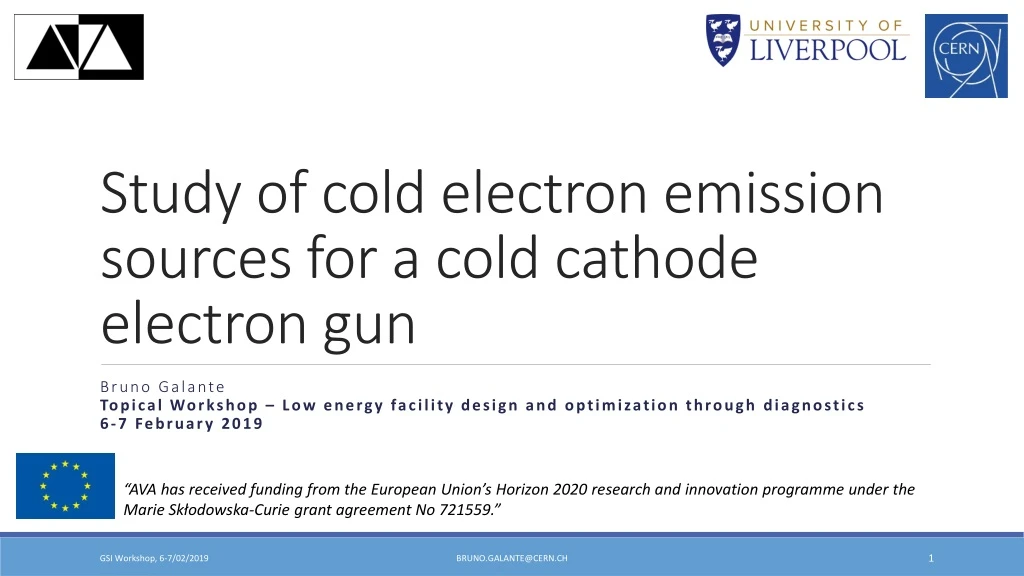
Study of cold electron emission sources for a cold cathode electron gun Bruno GalanteTopical Workshop – Low energy facility design and optimization through diagnostics6-7 February 2019 “AVA has received funding from the European Union’s Horizon 2020 research and innovation programme under the Marie Skłodowska-Curie grant agreement No 721559.” bruno.galante@cern.ch
Table of contents • ELENA and Electron cooling • Electron Cooler and Electron gun • Electron mission processes • Novel Emission Source • The Cold Cathode Test Bench • Results • Improvements & Next steps bruno.galante@cern.ch
ELENA [1][2] bruno.galante@cern.ch
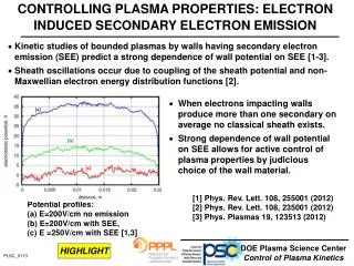
Electron Cooling • However, emittance blow-up is caused by: • Intra-beam scattering • Scattering with residual gases • Deceleration process. • Electron cooling reduces: • Longitudinal and Transverse energy spread (Momentum spread) • Size of the beam • Divergence of the ions Reaching thermal equilibrium between electrons and ions (e.g. antiprotons) in a time in the order of seconds. Result:A very intense and brilliant beam can be delivered to the experiments. [1][2][21] bruno.galante@cern.ch
E-Cooling Theory: a Brief Overview • Let’s consider an ion beam (in our case an antiproton beam) and an electron beam as 2 plasmas of different T. • High T Plasma:Ion beam - Low T Plasma:Electron beam. • If there is a big density of electrons and they are continuously generated, after a certain time Ion Beam T = Electron Beam T. • Electron-Ion interactions:Series of small-angle Rutherford scattering via Coulomb interaction where little momentum and energy is transferred. • Single ion-electron interaction: • • And the energy transferred from the ion to the electron would be: [1][2][21] bruno.galante@cern.ch
E-Cooling Theory: a Brief Overview Multiple collisions case.The effect of many scatters can be considered statistically using the statistical expectation value of the product of the momentum transfer components: Energy lost by the ion in the longitudinal direction - Cooling Force (frictional): Diffusion Coefficient: Rearranging: [1][2][21] bruno.galante@cern.ch
ELENA e-Cooler Electron Gun Collector ELENA Beam Cycle [3] bruno.galante@cern.ch
Electron Gun It must produce a • Cold (T⊥ < 0.1eV, T// < 1meV) • Intense electron beam (ne ≈ 1.5x1012 cm-3) Thermionic cathodes limit the performance of electron cooling due to high transverse Tof the emitted beam. Adiabatic expansion. Requires additional solenoid to generate a large magnetic field at the gun. Photocathodes suffer of an usually quite low lifetime, stability issues and are quite complicated to operate. Alternative solution: Field Emission due to have a Cold Cathode. E-Gun and Adiabatic expansion Effect of the expansion solenoid on the longitudinal field inside the drift solenoid [3] bruno.galante@cern.ch
Electron Gun It must produce a • Cold (T⊥ < 0.1eV, T// < 1meV) • Intense electron beam (ne ≈ 1.5x1012 cm-3) Thermionic cathodes limit the performance of electron cooling due to high transverse Tof the emitted beam. Adiabatic expansion. Requires additional solenoid to generate a large magnetic field at the gun. Photocathodes suffer of an usually quite low lifetime, stability issues and are quite complicated to operate. Alternative solution: Field Emission due to have a Cold Cathode. Effect of the expansion solenoid on the longitudinal field inside the drift solenoid [3] bruno.galante@cern.ch
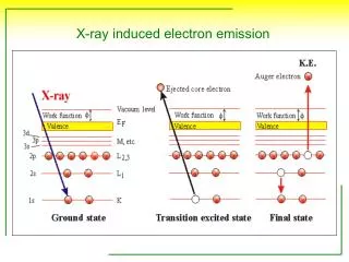
Field Emission Thermionic Emission, Photoemission: Generation of electronsonce the electrons have energy enough to overtake the potential barrier. Field Emission: Tunneling of electrons through the barrier applying a very large electric field (~ 107 V/cm). Fowler-Nordheim Theory. Number of electrons incident on a surface of unit area per unit time: And hence the current I is: And in field emission conditions, hence at low T: W: kinetic energy of the electron moving in direction normal to the surfaceF: Electric Field, k2=8π2m/h2 = 0, x <0. [4][5][6] bruno.galante@cern.ch
Carbon Nanotubes • For flat surfaces the required electric field is too strong. • Possible solution: Field Enhancement with tips Multi-Walled carbon NanoTube (MWNT) • PRO: • High aspect ratio -> High enhancement • Emit at low field, in order of some V/μm • Scalable production techniques • Chemical inertness and stable structure • CONS: • Small emitted current per tip • Screening effects • Impurities and defects Single-Walled NanoTube (SWNT) [4][5][6][7][8][9] bruno.galante@cern.ch
Vertically Aligned CNTs Best field emission performances have been achieved with perfectly aligned CNTs. However, several parameters have to be taken into account: • Screening Effect: Uniform penetration of the electric field is complicated for high density forests. Minimization and dense enough forests S= between 2h and 3h • Length distribution and burn-out Conditioning • Degradation MWNTs show better stability Effect of nanotubes density on the field emission performances Uniformity of the electric field on the carbon nanotubes forest and edge effect Screening effect in a COMSOL simulation. [10][11] bruno.galante@cern.ch
CNT Arrays Probably best solution to enhance FE performance. Also, more studies are present regarding these structures Growth Methods: • PECVD (Plasma-Enhanced Chemical Vapor Deposition) and TCVD (Thermal CVD) are the methods mostly used • Patterning via use of catalyst (e.g. Fe, Ni) with different shapes on the substrate. Parameter to optimize: • Spacing • Size of the forests. In Fig. above -> 30µm x 30µm Fe catalyst pattern at pitch distance 125 µm. Best performance achieved: 80 mA/cm2 at about 3 V/µm In Fig. below -> 1 mA/cm2 at 1,5 V/µm and current densities up to 1,5 A/cm2. h SEM images. 1 - Array of squared island of nanotubes. 2 - A single island. a, b - Array with hexagonal pattern. c – cross-section image. d – TEM image. e – CNT forest. f – Field simulation. [12][13] bruno.galante@cern.ch
CNT Arrays Probably best solution to enhance FE performance. Also, more studies are present regarding these structures Growth Methods: • PECVD (Plasma-Enhanced Chemical Vapor Deposition) and TCVD (Thermal CVD) are the methods mostly used • Patterning via use of catalyst (e.g. Fe, Ni) with different shapes on the substrate. Parameter to optimize: • Spacing • Size of the forests. In Fig. above -> 30µm x 30µm Fe catalyst pattern at pitch distance 125 µm. Best performance achieved: 80 mA/cm2 at about 3 V/µm In Fig. below -> 1 mA/cm2 at 1,5 V/µm and current densities up to 1,5 A/cm2. Outgassing and pressure control have to be carefully taken into account. a, b - Array with hexagonal pattern. c – cross-section image. d – TEM image. e – CNT forest. f – Field simulation. [12][13] bruno.galante@cern.ch
Exotic Structures • Doping:Modification of the crystalline structure introducing different elements, e.g. N, O. • Decoration:Metal coating using different metals with lower work function. • Composite Structures: Add of different structure on the top of the nanotubes to modify work function and/or increase enhancement factor. Illustration of doped CNTs. Effect of decoration with different elements on the FE performances. Composite structure: Few-Layer Graphene on the top of Carbon nanotubes [14]-[20] bruno.galante@cern.ch
Cold Cathode Test Bench Flange with 3 different CNT arrays Vacuum tank with the flange mounted in front bruno.galante@cern.ch
Cold Cathode Test Bench • The first test bench has been designed to characterize: • Necessary Conditioning process • Emitted current in function of the applied electric field • Stability of the emitted current • Lifetime Molybdenum Anode Carbon Nanotubes (CNT) Ceramic spacer bruno.galante@cern.ch
Conditioning Test 0.91 V/µm 1.94 V/µm 2.51 V/µm 1.48 V/µm 2.4 V/µm 2.63 V/µm bruno.galante@cern.ch
Fowler-Nordheim Plot Determination of material parameters and enhancement factor: “a” and “b” are necessary parameters for simulation of field emission. bruno.galante@cern.ch
Further Improvements & Next steps • Improvements: • Annealing of samples at 450 degrees in Ammonia atmosphere • Bake-out of the test bench • Resistor in series with the power supply Ballast Resistor • Next: • Measurement of Longitudinal and Transverse Energy depending on the inter-electrode distance bruno.galante@cern.ch
Cold Cathode Test Bench 2 • Allows measurements of: • Longitudinal Energy • Transverse Energy of the electron beam depending on the inter-electrode distance. • Longitudinal Energy: • Deceleration of the electron applying an inverse electric field. • Transverse energy: • Measure of the emission spot on a phosphor screen. Linear Motion Feedthrough Support for CNT Extracting Grid Anode (not present in the reality) bruno.galante@cern.ch
Thank you “AVA has received funding from the European Union’s Horizon 2020 research and innovation programme under the Marie Skłodowska-Curie grant agreement No 721559.” bruno.galante@cern.ch
References • [1] - https://espace.cern.ch/elena-project/SitePages/Home.aspx[2] - ELENA: the extra low energy anti-proton facility at CERN – S.Maury, W.Oelert, W.Bartmann, P.Belochitskii, H.Breuker, F.Butin, C.Carli, T.Eriksson, S.Pasinelli, G.Tranquille[3] - The ELENA electron cooler: parameter choice and expected performance – G.Tranquille, A.Frassier, L.Joergensen[4] - Electron emission in intense electric fields – R.H.Fowler, Dr.L.Nordheim[5] - Carbon Nanotube Electron Source: from electron beams to energy conversion and optophotonics – AlirezaNojeh[6] - Electron field emission from carbon nanotubes – Y.Cheng, O.Zhou[7] - Vacuum nanoelectronics devices: Novel electron sources and applications – A. Evtukh, H. Hartnagel, O. Yilmazoglu, H. Mimura, D. Pavlidis[8] - Carbon nanotubes for cold electron sources – P.Groning, P.Ruffiex, L.Schlapbach, O.Groning[9] - Carbon Nanotube and related field emitters: Fundamentals and applications – Yahachi Saito [10] - Array geometry, size and spacing effects on field emission characteristics of aligned carbon nanotubes – Y.M.Wong, W.P.Kang, J.L.Davidson, B.K.Choi, [11] - Maximizing the electron field emission performance of carbon nanotube arrays – R.C.Smith, S.R.P.Silva[12] - Patterned selective growth of carbon nanotubes and large field emission from vertically well-aligned carbon nanotube field emitter arrays – J.Sohn, S.Lee, Y.-H.Song, S.-Y.Choi, K.-S.Nam[13] - High emission current density, vertically aligned carbon nanotube mesh, field emitter array – C.Li, Y.Zhang, M.Mann, D.Hasko, W.Lei, B.Wang, D.Chu, D.Pribat, G.Amaratunga, W.I.Milne[14] - The doping of carbon nanotubes with nitrogen and their potential applications – P.Ayala, R.Arenal, M.Rummeli, A.Rubio, T.Pichler[15] - Oxygen and nitrogen doping in single wal carbon nanotubes: An efficient stable field emitter – A.Kumar, S.Parveen, S.Husain, M.Zulfequar, Harsh, M.Husain[16] - Improved field emission properties of carbon nanotubes decorated with Ta layer – Z.Wang, Y.Zuo, Y.Li, X.Han, X.Guo, J.Wang, B.Cao, L.Xi, D.Xue[17] - Highly improved field emission from vertical graphene-carbon nanotube composites – J.-H. Deng, R.-N. Liu, Y.Zang, W.-X. Zhu, A-L.Han, G.-A. Cheng[18] - Highly improved field emission from vertical graphene-carbon nanotube composites – J.-H. Deng, R.-N. Liu, Y.Zang, W.-X. Zhu, A-L.Han, G.-A. Cheng [19] - Enhanced field emission properties of a reduced graphene oxide/carbon nanotube hybrid film – D.D.Nguyen, Y.-T.Lai, N.-H.Tai[20] - Excellent field emission characteristics from few-layer graphene-carbon nanotube hybrids synthesized using radio frequency hydrogen plasma sputtering deposition – J.-H.Deng, R.-t. Zheng, Y.-M.Yang, Y.Zhao, G.-A.Cheng[21] – Electron cooling: Theory, Experiment, Application – Helmuth Poth bruno.galante@cern.ch
Adiabatic Expansion • Single electron case. If:- axially symmetric field geometry, B = B‖(z)- electron moves slowly enough • We can consider the following adiabatic invariance: • When the field is reduced from the value Bi to a value B: • Also, the magnetic flux contained in the cross section of the assumed cylindrical electron beam is an adiabatic invariant, therefore it will increase when the B decreases: • Multiple electrons. For multiple, not independent electrons, the Coulomb interaction breaks the invariance. However, the invariance stands for the average transverse energy: • Therefore: Electron cooling and recombination experiments with an adiabatically expanded electron beam – S.Pastuszka, U.Schramm, M.Grieser, C.Broude, R.Grimm, D.Habs, J.Kenntner, H.-J.Miesner, T.Schussler, D.Schwalm, A.Wolf bruno.galante@cern.ch
Fowler-Nordheim Plot bruno.galante@cern.ch
SEM of CNT Array bruno.galante@cern.ch
Longitudinal and Transverse Energy ~ -2kV ~ -2kV Longitudinal Energy Transverse Energy r Starting from: 2) TE ~ +1kV 0 to ~ -2kV 1 - The Commissioning of TESS: An experimental facility for measuring the electron energy distribution from photocathodes – L.B. Jones, R.J. Cash, B.D. Fell, T.C.Q. Noakes, B.L. Militsyn2 - Electron transverse energy distribution in GaAs negative electron affinity cathodes: calculations compared to experiments – G.Vergara, A. Herrera-Gomez, W.E. Spicer bruno.galante@cern.ch
Grid vs Hole Grid Hole bruno.galante@cern.ch
Grid Effect Grid No Grid bruno.galante@cern.ch