Download
1 / 21
210 likes | 379 Views
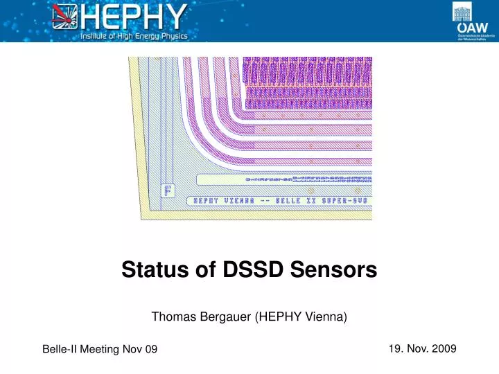
Status of DSSD Sensors. Belle-II Meeting Nov 09. Overview. Prototype DSSDs have been ordered at Hamamatsu (rectangular shape) Micron Semiconductor (wedge shape) I will present status of both orders. SVD Layout. Hamamatsu Order. RECTANGULAR SENSORS. Hamamatsu Status.

E N D
Status of DSSD Sensors Thomas Bergauer (HEPHY Vienna) Belle-II Meeting Nov 09
Overview • Prototype DSSDs have been ordered at • Hamamatsu (rectangular shape) • Micron Semiconductor (wedge shape) • I will present status of both orders Thomas Bergauer (HEPHY Vienna)
SVD Layout Thomas Bergauer (HEPHY Vienna)
Hamamatsu Order RECTANGULAR SENSORS Thomas Bergauer (HEPHY Vienna)
Hamamatsu Status • HPK decided to re-start DSSD production • Not only for Belle. They have been pushed also from other interested (Japanese) parties • KEK was in contact with Japanese sales representative and engineer • Beginning of Oct. 2009: Mask Production • Unfortunately without the possibility to add test structures • Delivery: March 2010 (<=30pcs.) Thomas Bergauer (HEPHY Vienna)
Rectangular DSSD Layout • Overall Size: • 124.88 x 59.6 mm • P-side • 768 long readout strips • 75 micron readout pitch • 37.5 micron strip pitch(one intermediate strip) • Second row of bonding pads compatible to Origami bonding scheme • N-side • 512 short readout strips • 240 micron readout pitch • 120 micron strip pitch(one intermediate strip) Thomas Bergauer (HEPHY Vienna)
Rectangular DSSD Specifications Thomas Bergauer (HEPHY Vienna)
Micron Order WEDGE SENSORS Thomas Bergauer (HEPHY Vienna)
Micron Semiconductor Ltd. • Company in Sussex, England, founded 1983 • Contact persons: • Colin Wilburn (Director) • Susan Walsh (Designer) • Financial: (eq. 8M¥) Thomas Bergauer (HEPHY Vienna)
Wedge DSSD specifications • Resistivity: 8 kΩcm (n-type); crystal orientation <100> • Thickness: 300 +/- 10 microns • Full Depletion (FD): 40 volts typical; 70 volts maximum • Operating Voltage: FD to 2x FD • Minimum Breakdown Voltage (10uA): 2.5x FD • Total drain leakage current (20 degrees C): 2uA typical; 10uA maximum (at 50% rH) • Polysilicon resistor 15 +/- 5 megohms • Coupling capacitor > 1.2 pF / cm strip length and per microstrip width (100pF typical) • Interstrip resistance 100MΩ min, 1 GΩ ohm typical (P-Side);10 MΩ min, 100MΩ typical (N-side) Thomas Bergauer (HEPHY Vienna)
Micron Wafer Layout (to be confirmed) 3 different GCDsfor the n-side Quadratic baby sensors 2,3,4 p-side: 512 strips 50 µm pitch 1 interm. strip n-side: 256 strips 100 µm pitch 0 interm. strip different p-stop patterns Main sensor p-side: 768 strips 75-50 µm pitch 1 interm. strip n-side: 512 strips 240 µm pitch 1 interm. strip combined p-stop Teststructures for p-side 1) atoll p-stop varying distance from strip 2) conventional p-stop varying width 3) combined p-stop varying distance from strip Baby sensor 1 p-side: 512 strips 50 µm pitch 1 interm. strip n-side: 512 strips 100 µm pitch 1 interm. strip atoll p-stop Teststructures for n-side(no GCD) Thomas Bergauer (HEPHY Vienna)
Open Points: Guard Ring Design • We proposed single guard ring with outer n-ring (n_sub) similar to HPK design • 800 micron size • Micron wants to implement their own multi-guard ring design • Three guard rings • 1000 micron size • Requires NDA signed by us • They do not like n_sub implant; however, this make IV tests more complicated Thomas Bergauer (HEPHY Vienna)
Open Points: p-stop layout combined p-stops connected p-stops isolated Thomas Bergauer (HEPHY Vienna)
Micron Wafer Layout (to be confirmed) 3 different GCDsfor the n-side Quadratic baby sensors 2,3,4 p-side: 512 strips 50 µm pitch 1 interm. strip n-side: 256 strips 100 µm pitch 0 interm. strip different p-stop patterns Main sensor p-side: 768 strips 75-50 µm pitch 1 interm. strip n-side: 512 strips 240 µm pitch 1 interm. strip combined p-stop Teststructures for p-side 1) atoll p-stop varying distance from strip 2) conventional p-stop varying width 3) combined p-stop varying distance from strip Baby sensor 1 p-side: 512 strips 50 µm pitch 1 interm. strip n-side: 512 strips 100 µm pitch 1 interm. strip atoll p-stop 1) 2) 3) Teststructures for n-side(no GCD) Thomas Bergauer (HEPHY Vienna)
Micron Wedge DSSD - Summary • One intermediate strip on both p-side and n-side • Outer dimensions: • Width on top: 60.15 ± 0.05 mm • Width on bottom: 40.60 ± 0.05 mm • Length: 125.11 ± 0.05 mm • Note: all dimension values are preliminary, i.e. they are subject to discussion and are awaiting final confirmation by Micron! Thomas Bergauer (HEPHY Vienna)
Schedule • Most urgent: agree on open points with Micron to start production as fast as possible • Wait for delivery • Hamamatsu: end of March 2010 • Micron: Summer 2010 Thomas Bergauer (HEPHY Vienna)
Future next steps with prototype DSSDs • Electrical Characterization in Vienna • Build Origami module with HPK sensors • Build full ladder comprising • several Origami modules • slanted module with Micron sensor • Testbeam in autumn 2010 at CERN • Irradiation tests of sensors • Together with electronics? • Where? When? Thomas Bergauer (HEPHY Vienna)
THE END. Thomas Bergauer (HEPHY Vienna)
P-Side, AC and DC pads Marker with 10 µm diameter (easily adjustable) on every 128th AC pad AC pads: 50 x 200 µm, 2 staggered rows DC pads: 42 x 108 µm 1 staggered row • As long as the pad pitch within each row is constant, different pitches in different pad rows do not cause problems for bonding. Thomas Bergauer (HEPHY Vienna)
N-Side, P-Stop pattern (implants only) Individual P-Stop atoll N+ implantof strip Additional P-Stop „strip“ splitting theaccumulation layer • According to Y. Iwata et al., this “combined pattern” performs best for a tradeoff between charge collection efficiency and interstrip capacitance. Thomas Bergauer (HEPHY Vienna)
N-Side, AC and DC pads • AC pad size: 260 x 60 µm, marker on every 128th pad, 2 rows, no staggering • DC pad size: 180 x 60 µm, 1 row, no staggering Thomas Bergauer (HEPHY Vienna)