Download
1 / 21
210 likes | 377 Views
IR CARBON NANO-TUBE TRANCIEVER . SDP team Yngvesson Ioan Tihenea Tomas Broka Dmitriy Stupak Sergey Derivolkov. Outline. Recap Design Overview System Overview Signal Processing Block (Transmitter End) Transceiver Signal Processing Block (Receiver End) Suspension Method

E N D
IR CARBON NANO-TUBE TRANCIEVER SDP team Yngvesson Ioan Tihenea Tomas Broka Dmitriy Stupak Sergey Derivolkov
Outline • Recap Design Overview • System Overview • Signal Processing Block (Transmitter End) • Transceiver • Signal Processing Block (Receiver End) • Suspension Method • Fabrication Techniques Used • Current Status and Group Breakup • Questions
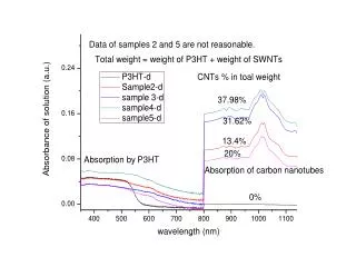
Recap Design Overview For our Senior Design Project we are working on creating a communication system that has two computer interface terminals, some signal processing at each end and an Infrared communication channel (transceiver) in the center. The key component to our SDP project is a Single Walled Carbon Nanotube (SWNT) thin film detector detecting IR radiation which changes the resistivity across it; this will be interpreted in binary values.
Outline • Recap Design Overview • System Overview • Signal Processing Block (Transmitter End) • Transceiver • Signal Processing Block (Receiver End) • Suspension Method • Fabrication Techniques Used • Current Status and Group Breakup • Questions
Outline • Recap Design Overview • System Overview • Signal Processing Block (Transmitter End) • Transceiver • Signal Processing Block (Receiver End) • Suspension Method • Fabrication Techniques Used • Current Status and Group Breakup • Questions
Signal Processing Block (Transmitter End) • Microcontroller • IR LED and Circuitry • Silicon Laboratories • SiLabs C8051F340 • USBXpress
Outline • Recap Design Overview • System Overview • Signal Processing Block (Transmitter End) • Transceiver • Signal Processing Block (Receiver End) • Suspension Method • Fabrication Techniques Used • Current Status and Group Breakup • Questions
Outline • Recap Design Overview • System Overview • Signal Processing Block (Transmitter End) • Transceiver • Signal Processing Block (Receiver End) • Suspension Method • Fabrication Techniques Used • Current Status and Group Breakup • Questions
Signal Processing Block (Receiver End) • Amplifier and Comparator • Circuitry for clean pulses • Microcontroller
Outline • Recap Design Overview • System Overview • Signal Processing Block (Transmitter End) • Transceiver • Signal Processing Block (Receiver End) • Suspension Method • Fabrication Techniques Used • Current Status and Group Breakup • Questions
Suspension Method • Fabrication of Supporting Washer • Electrical Contacts • Connecting SWCN Film to Supporting Washer
Outline • Recap Design Overview • System Overview • Signal Processing Block (Transmitter End) • Transceiver • Signal Processing Block (Receiver End) • Suspension Method • Fabrication Techniques Used • Current Status and Group Breakup • Questions
Fabrication Techniques Used • Plasma etching premade film • Film was placed in oxygen plasma to etch down to required thickness. • Vacuum filtration method • Pour CNT solution onto membrane and vacuum non-CNT liquid out. Then dissolve membrane. • Dry drop method • Place electrical contacts on glass slides and putting drops of the CNT solution between them.
Outline • Recap Design Overview • System Overview • Signal Processing Block (Transmitter End) • Transceiver • Signal Processing Block (Receiver End) • Suspension Method • Fabrication Techniques Used • Current Status and Group Breakup • Questions
Group Breakup Sergey Derivolkov, EE: • Designed the system overview and helped provide more efficient procedures for the fabrication. Also used SEM to take pictures of the NanoComp film and measured the thickness. Dmitriy Stupak, EE: • Designed the circuitry to test the film resistivity and the effects of IR radiation. He also joined Ioan during plasma etching procedure and used Profilometer to measure the thickness of the etched film. Tomas Broka, CSE: • Worked on fabrication procedure for the first couple films. Tomas also set up the website of the team and he is in charge of ordering components, equipment, and keeps contacts up to date through emails and through the website. Also he worked with SEM to take images. Ioan Tihenea, EE: • Worked on plasma etching procedure for the film offered by NanoComp. He used Atomic Force Microscope (AFM) to take images of the films surface. He also was involved as well as Tomas in the fabrication.
Outline • Recap Design Overview • System Overview • Signal Processing Block (Transmitter End) • Transceiver • Signal Processing Block (Receiver End) • Suspension Method • Fabrication Techniques Used • Current Status and Group Breakup • Questions