Download
1 / 20
210 likes | 498 Views
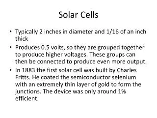
Solar Cells --- frontiers in materials and devices. Ning Su. Outline. Introduction Market & technology comparison Low cost solar cells thin film solar cells (TFSC) High efficiency solar cells Advanced Si solar cells Tandem cells Thermophotovoltaic

E N D
Solar Cells --- frontiers in materials and devices Ning Su EE 666 Advanced Semiconductor Devices
Outline • Introduction • Market & technology comparison • Low cost solar cells • thin film solar cells (TFSC) • High efficiency solar cells • Advanced Si solar cells • Tandem cells • Thermophotovoltaic • other strategies • Conclusions EE 666 Advanced Semiconductor Devices
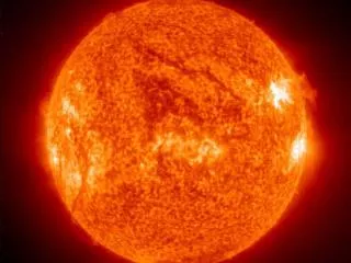
Introduction • Why PV ? • Average power incident upon continental United states is ~ 500 times of national energy consumption ( total, not just electricity) • Environmentally-friendly renewable energy source • Quiet • Reliable • Applications • Residential Cost-effective way to provide power to remote area • Space applications satellite, space stations EE 666 Advanced Semiconductor Devices
Photovoltaic Cells, Modules and Systems • Solar cell is the basic building blocks of solar PV • Cells are connected together in series and encapsulated into models • Modules can be used singly, or connected in parallel and series into an array with a larger current & voltage output • PV arrays integrated in systems with components for charge regulation and storage Cell module array system EE 666 Advanced Semiconductor Devices
Market for Solar PV • PV market grows at fast rate especially in recent years • Cumulatively, about 2GW of solar cells are being used in a variety of applications EE 666 Advanced Semiconductor Devices
Comparison of PV Technology World PV module production in 2003 • main technologies available: single & multi- cystalline Si, a-Si, CuInSe2, CdTe…. • Bulk cystalline Si remains dominant • Different technology comparison in efficiency & cost EE 666 Advanced Semiconductor Devices
Low Cost vs. High Efficiency SC Applications: Space Terrestrial Demands: Low cost High efficiency High efficiency Light weight Radiation resistance Technology: Thin film Organic SC tandem TPV Materials: Multicystalline Si III-V Single crystalline Si a-Si ; CIS; CdTe EE 666 Advanced Semiconductor Devices
Thin Film Solar Cells • “thin film” refers more to solar cell technologies with mass-production possibilities • Rather than the film thickness. • requirement for suitable materials: low cost, high absorption, doping, transport, robust and stable leading materials for TFSC: CdTe, CuInSe2, (CIS) ,a-SI… • advantages: -- low material requirement -- variety of processing methods -- light weight modules • disadvantages: -- low achieved efficiency EE 666 Advanced Semiconductor Devices
CIS & CdTe TFSC • CIS, direct band gap with Eg~ 1eV, α>105 cm-1 • high cell efficiency (19.2 %), model efficiency (13.4%) • comparatively long lifetime • Current complicated and capital intensive fabrication • CdTe, direct band gap with Eg~ 1.45eV, α>105 cm-1-- ideal suited for PV applications • Record cell efficiency 16.5 % (NREL) • Numerous promising processing techniques EE 666 Advanced Semiconductor Devices
Solar Cell Efficiency • Ideal cell efficiency • Effect of bandgap on efficiency • GaAs, InP have Eg close to the optimum, favored for high η cells • Si less favorable Eg but cheap & abundant • Effect of spectrum on efficiency • improving η by concentrating light 100 suns or more illumination Parabolic reflector Fresnel lens EE 666 Advanced Semiconductor Devices
Rear metal reflector Minimize Losses in Real SC • Optical loss • Concentration of light • Trapping of light: • AR coatings • Mirrors ( metallization rear surface or growing active layers on top of a Bragg stack) • textured surface • Photon recycling reabsorption of photons emitted by radiative recombination inside the cell Double path length in metallized cell • Electrical loss • Surface passivation • Resistive loss …… EE 666 Advanced Semiconductor Devices
Advanced Si Solar cells Crystalline Si efficiency PERL cell • large improvement in the last 15 years 1) textured surface & AR coating 2) Improved surface passivation • PERL cell ( 24% in 1994 ) • Buried contact cell commercialized by BP Solarex advantage: fine grid– reduced shading–Jsc reduced contact recombination – Voc series resistance – concentrator sc Burried contact sc • Martin A. Green etc.,” Very high efficiency silicon solar cells-science and technology,” IEEE Trans. Electron • Devices,vol. ED-46,pp1940-47,1999. EE 666 Advanced Semiconductor Devices
Tandem Cells – beyond efficiency limit • Concept • Intrinsic efficiency limit using single semiconductor material is 31% • Stack different band gap junctions in series larger band gap topmost • efficiency of 86.8% calculated for an infinite stack of independently operated cells * * A. Marti, G. L. Araujo, Sol. Energy Mater. Sol. Cells 43 (1996) 203. EE 666 Advanced Semiconductor Devices
Tandem Cells -- Practical approaches • Advantages : high efficiency • Cover wider range of solar spectrum • reduce thermerlisation loss (absorbed photon with energy just little higher than Eg) • Practical approaches • individual cells grown separately and mechanically stacked • monolithically grown with a tunnel-junction interconnect EE 666 Advanced Semiconductor Devices
GaInP/GaAs/Ge Dual- and triple-junction SC • Dual-junction (DJ) • GaInP/GaAs cells on Ge (average AM0 η 21.4 %) * • small-area lab cells large-scale manufacturing approach megawatt level ** • Triple-junction (TJ) • efficiency of 27.0% under AM0 illumination at 28 0C * * N. H. Karam etc. Solar Energy Materials & Siolar cells 66 (2001) 453-466. **N. H. Karam etc. Trans. Electron Dev. 46 (10) 1999 pp.2116. EE 666 Advanced Semiconductor Devices
Multiple Junction Cells • Four-junction cells under development • addition of 1-eV GaInNAs subcells under GaAs to form 4 junctions • InGaN – potential material for MJ cells • Direct energy gap of InGaN cover most of the solar spectrum* • MJ solar cells based on this single ternary could be very efficient * LBNL/Conell work: J. Wu et al. APL 80, 3967 (2002). EE 666 Advanced Semiconductor Devices
Thermophotovoltaic (TPV) • TPV solar energy conversion Photovoltaic conversion with the addition of an intermediate thermal absorber/emitter is known as thermophotovoltaic (TPV) energy conversion. Solar radiation is used to heat absorber/emitter to temperature of 1200-2500 K emitter radiates photons PV cell converts the energy of radiation into electrical power. • Advantage By matching the spectrum of the emitter to the PV cells, efficiency improved. EE 666 Advanced Semiconductor Devices
TPV Configuration • Components of a TPV system All TPV systems include: 1) heat source 2) radiator 3) PV converter 4) means of recovering unusable photons Selective emitter matched to PV cells EE 666 Advanced Semiconductor Devices
Other Strategies – for high efficiency • Intermediate band solar cells • A.Luque and A. Marti,”Increasing the effiency of ideal solar cells by photon • Induced transitions at intermediate levels”, Phys. Rev. Lett. 78, 5014 (1997) • Low-dimentional strucutrues, QWs, QDs • Impact ionization solar cells • P. Wueerfel, “Radiative efficiency limit of terrrestrial solar-cells with internal carrier multiplication”, Appl. Phys. Letts. 67, 1028 (1995). • Hot carrier solar cells • P. Wueerfel, “Radiative efficiency limit of terrrestrial solar-cells with internal carrier multiplication”, Appl. Phys. Letts. 67, 1028 (1995). …… EE 666 Advanced Semiconductor Devices
Conclusions • Remarkable progress made in synthesis, processing and characterization leads to major improvement in PV efficiency and reduction in cost • Silicon continues to dominate the PV industry • Thin film and organic solar cells offer promising options for substantially reducing the cost, competitive for terrestrial applications • Very high efficiency achieved in multiple junction III-V semiconductors presently commercialized for space applications • New device concept for high efficiency facing challenges and prospects EE 666 Advanced Semiconductor Devices