Download
1 / 16
160 likes | 179 Views
Detailed overview of CSC EMU Muon Port Card (MPC) functionality, data formats, FPGA mezzanine board, VME interface, clock options, and testing up to date including standalone tests, beam tests, and irradiation tests. Also, explore plans for MPC production and testing.

E N D
CSC EMU Muon Port Card (MPC) Status Plans M.Matveev Rice University August 27, 2004
Overview • Functionality - Data formats - FPGA mezzanine board and firmware - VME interface - Clock options • Tests done up to date - Standalone tests - Tests of the TMB and SP interfaces - Beam test - Irradiation test • Plans for MPC production and testing - Cost Estimate - Schedule
D M B T M B D M B T M B D M B T M B D M B T M B D M B T M B C C B M P C T M B D M B T M B D M B T M B D M B T M B D M B C O N T R O L L E R 1 of 5 1 of 5 CFEB CFEB CFEB CFEB CFEB 1 of 2 1 of 24 ALCT LVDB Anode Front-end Board CSC CSC EMU/Trigger Electronics Muon Portcard (1) Trigger Motherboard (9) Clock Control Board DAQ Motherboard (9) 3 optical links CSC PeripheralCrate (60) On the periphery of the return yoke Muon Sorter (1) Sector Processor (12) CSC Track-Finder Crate (1) In underground counting room On detector
Functionality • One board per CSC sector, resides in the middle of the peripheral EMU crate • Receives up to 2 LCTs from each of 9 Trigger Motherboards over custom backplane (8 TMB for station 1) • Does sorting “3 out of 18” (or “2 out of 16”) LCTs based on 4-bit “Quality” pattern • Transmits 3 best LCTs in ranked order to Sector Processor over optical cables
TMB – to – MPC – to - SP Data Format • Same data format for TMB-to-MPC and MPC-to-SP communication • Data is transmitted in two frames at 80Mhz
80Mhz Clock Options • TLK2501 Gigabit serializers need 80Mhz reference clock: - 80.16Mhz clock directly from QPLL on CCB’2004 board (dedicated LVDS pair on custom backplane) - ICS AV9170-1 clock multiplier (40.08Mhz x 2) Both options will be implemented, assuming the 80.16Mhz direct clock from QPLL to be the primary choice
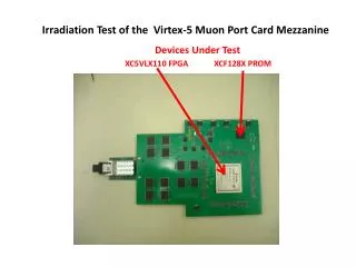
FPGA Mezzanine Card • Based on Xilinx XCV600E-8FG680C FPGA + XC18V04 EPROM • Have 64 mezzanines assembled and tested at UCLA + 6 old mezzanines on existing MPC prototypes
Firmware • 9 links from Trigger Motherboards, 9x32=288 inputs @ 80Mhz • 3 links to TLK2501 serializers, 3x16=48 outputs @ 80Mhz • 1 status link (“winners”) to TMB’s, 9 outputs @ 80Mhz • VME and CCB interfaces, ~75 inputs and outputs • Input and output FIFO buffers for testing purposes
Assembled Board Power +5V: < 1A +3.3V: < 2A Board latency = 115 ns
Current Status and Tests • 6 boards were built in 2002, all equipped with FPGA mezzanines • Have been tested on the bench (next slides) • Have been tested with 7 Trigger Motherboards and one Sector Processor (next slides) • Have been checked in the peripheral crates at the beam test at CERN in September 2003 and June 2004 (next slides) • Have been tested under irradiation at UC Davis cyclotron (next slides)
Standalone Tests of MPC • Have developed software to test the MPC in any (peripheral or Track Finder) crate with any (CCB’2001 or CCB’2004) Clock and Control Board • What was tested: VME interface sorting logic - load test patterns into input FIFO - run them through the sorter - check sorting result from the output FIFO EPROM programming/verification from VME Reconfiguration from EPROM on Hard Reset • Results > 2M iterations of FIFO-to-FIFO test (sorter logic) without errors
MPC Test with TMB’s and SP • Clock and commands are coming from TTCvi/vx through CCB’2004 • Load 255 words (510 frames) of data into output FIFO of 7 TMB’s • Pass these patterns through the MPC to SP at 80Mhz • Check data from: - MPC output FIFO - SP input FIFO - TMB “winner” RAM Results • Ran >2M test iterations without errors (BER < 10-9) • Measured the “safe” window of data latching on MPC inputs (~5 ns) • Have found several broken “thin” optical cables. “Thick” cables are more reliable
Beam Test at CERN, June 2004 • During unstructured beam one MPC was receiving LCTs from 4 Trigger Motherboards and sending 3 best patterns to SP • During structured beam two MPCs were receiving LCTs from two Trigger Motherboards each and sending selected patterns to one or two SP’s Both clocking solutions were checked No link errors detected Compare trigger data vs DDU data. Mismatches detected in specific runs and specific chambers. Likely to be an issue with DAQ path for TMB <0.25% mismatches in “winner” bits, mostly due BX mis-assignment See http://www.phys.ufl.edu/~acosta/tb/talks/csctb04_sp_results.pdf for more info
Irradiation Test of the MPC • TLK2501 gigabit transceivers, two devices were tested Irradiated up to 270 kRad, no SEL, 12(19) SEU • Finisar FTRJ-8519 –1-2.5 optical transceiver, two devices were tested No errors up to 70 kRad, both failed permanently at 70 kRad • Xilinx EPROM XC18V04 Irradiated up to 7 kRad, 1 error during read back over JTAG, but configuration wasn’t changed and FPGA was successfully reloaded • Xilinx XCV600E-8FG680C FPGA Irradiated up to 2.3 kRad SEU occurred on average after a fluence of 108 p/cm2 (15 rad for Si) FPGA would always recover after a Hard Reset • Discrete logic Same CMOS families as on TMB, DMB, CCB boards No damage observed
Production and Testing Plans • Need to make ~20 changes in schematic/layout, add 4-5 small chips to VME interface. List of changes is being prepared • Design documentation is available on the web at http://bonner-ntserver.rice.edu/cms/projects.html#mpc, including - specification - schematics - configuration file for EPROM • 70 MPC motherboards will be built and assembled (including 15% spare) - will order ~5% more components for future repairs • In-house testing (Matveev, Lee, Tumanov) - will use two crates and run testing patterns from TMBs through MPC to SP - software is under development (including convenient GUI) • Burn in 24 hours at 60..70 C then test again (intend to use OSU oven)
Cost Estimate and Production Plans MPC main board • Components …………………………………………… $1025 x 70 = $71,750 • Services (PCB & front panel fabrication, assembly)... $500 x 70 = $35,000 Mezzanine card • Components and services for 70 cards (assembly, test at UCLA) ... $65,970 Total………… $172,720 Make schematic/layout changes and build 3 sample boards… Oct - Dec 2004 Order all components …………………………………………. Oct - Dec 2004 Assemble/Test 3 sample boards ………………………………. Jan - Feb 2005 Need to test this sample with 9 TMB’s in the production peripheral crate If OK fabricate the rest 67 boards ……………………………. March 2005 Assemble and test 67 boards ………………………………….. April – Aug 2005
![AE = [ W + Y e – PL – r – mpc ∙ T + I + G + X ] + { mpc – mpm } Y](https://cdn1.slideserve.com/2599389/slide1-dt.jpg)