Download
1 / 22
220 likes | 327 Views
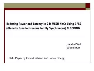
Reducing Power and Latency in 2-D MESH NoCs Using GPLS (Globally Pseudochronous Locally Synchronous) CLOCKING. Harshal Ved 200501020 Ref:- Paper by Erland Nilsson and Johny Oberg . Introduction. In high performance VLSIs, clock net is the cause of two problems :-

E N D
Reducing Power and Latency in 2-D MESH NoCs Using GPLS (Globally Pseudochronous Locally Synchronous) CLOCKING Harshal Ved 200501020 Ref:- Paper by Erland Nilsson and Johny Oberg
Introduction • In high performance VLSIs, clock net is the cause of two problems :- • It is a major source for power consumption . • Keeping Clock skews within tolerable limits is a design bottleneck. • Solution :- • Partition the design into large synchronous blocks that communicate globally asynchronously using handshake signals[1].
Previous Work • Three ways to reduce power consumption :- • Reducing Voltage • Reducing Physical Capacitance • Reducing Activity • Third category is seen as having great potential for the purpose .
2-D mesh NoC • Example of a 2-D mesh NoC showing Switches (S) and Resources (R) with their interconnections.
Approximately 70% of the power is burned in clock distribution and Latches [2] . • Solution to above problem :- • GALS (Globally Asynchronous Locally synchronous) clocking. • Mesochronous clocking .
Drawbacks of Globally synchronous operations [3] • Large Peak current at clock edge, leading to ground bounce and voltage drops, which in turn induce jitter in both clock and data. • Very difficult to match the delay in different braches of global tree. • Globally synchronous systems are not scalable.
GALS (Globally Asynchronous Locally synchronous) • GALS architecture is composed of large synchronous blocks which communicate with each other on an asynchronous basis but communicate internally on synchronous basis. • Disadvantage with GALS :- • The asynchronous communication between the clock regions must be controlled with handshake regions. This leads to reduced maximum frequency and an increased area overhead. • Limitations in availability of design tools .[3] • Lack of global clock level. [4]
Mesochronous Clocking [3] • Mesochronously clocked systems employ a single clock across the entire system, but at an arbitrary phases. • Advantages :- • Power dissipation in the clock distribution network is significantly reduced . • Mesochronous systems are scalable . • Disadvantage :- • Nothing can be said concerning the phase alignment between clocks in different parts of the system. • Thus metastability may occur when passing data between clock phase domains.
GPLS (Globally Pseudochronous Locally synchronous) • Pseudochronous is for short for pseudo-synchronous which is mesochronous clock with constant phase difference between local clock regions. • Distribution of clock is done between the switches. Limitation:- • In both the cases i.e. GPLS and Mesochronous clocking system, the clock distribution layout benefits only if there is regular topology with constant distance between each node/region .
GPLS Vs Mesochronous • For Mesochronous NoC, data is forwarded without any concern of phase. • If clock arrives (almost) simultaneously with data, there might be problem with metastability with latches. • In the pseudochronous case, both the frequency and the phase are constant. If we select the phase constant carefully, we can guarantee that data always arrive slightly before the clock for some paths.
Pseudochronous NoC Clocking • Every switch has four outgoing and four incoming connections to the surrounding switches and is able to switch packets in all four directions in one cycle. • The network uses hot-potato routing and a complete 128 bit packet is sent in parallel in one clock cycle. Hot-potato routing leads to that no packet is queued in a switch if the output that aims towards the destination is not available. • By selecting the phases of the switch nodes, the communication in certain paths is made with lower latency compared to a case if every switch had identical phase. We call such path a data motorway (DM).
The phase difference w.r.t. the reference clock, i.e. the clock source, is increased every time the clock is forwarded to the next node. • The clock period is divided into M phases which gives the minimum phase difference. • For example, M = 4 means that fourdifferent phases are used across the chip, M = 1 is equivalent to the synchronous case.
Example of clock distribution for 4X4 mesh with four constant phases (M=4) • Phase difference between two neighbouring switches is given by:- m (T∆/Tperiod)
Power Analysis • There are two issues when it comes to reducing the power consumption • Reducing the average power consumption. • Reducing the peak power consumption.
Average Power Analysis • Reducing the average power means that the overall power consumption is reduced, i.e., less energy is spent per clock cycle. • The power consumption of a block of random logic with n gates can be estimated as Pavg = (Ksw.n.Cld.Vp^2)/tclk • Since the average power is dependent on the frequency and the amount of logic, the only affect our clock phasing scheme can have on a design is how the clock is distributed, i.e., if it reduces the amount of switched capacitance on the clock wires.
Peak Power Analysis • Reducing the Peak power means that the amount of by-pass capacitance that is needed on-chip to even out the switching current can he reduced. • Local bypass capacitances are placed closed to the gates to counter power supply noise. • Extra capacitances deliver extra current. Thus, reducing peak power reduces the power supply noise and thus the clock jitter in the circuit. [5]
Peak Power Analysis Peak Power triangles, a) single peak h) two peakswith a phase difference, e) two peaks with a phase difference of180 degrees (M=2), d) four peaks with a phase difference of 90degrees (M=4).
Conclusions: • In GPLS clock distribution peak power is halved which is nearly equal to the average power. • The power supply noise and clock jitter have been reduced. • Another benefit by forwarding the clock over data lines is that it can save one metal layer that traditionally is used for global clock distribution.
References • [1] http://citeseer.ist.psu.edu.html • [2] C. Anderson. Physical design of a fourth-generation POWER GHz microprocessor. In Solid-State Circuits Conference, 2001. • [3] Tobias Bjerregaard, A Scalable, Timing-Safe, Network-on-Chip Architecture with an Integrated Clock Distribution Method. • [4] T. Bjerregaard and J. Sparsø. A scheduling discipline for latency and bandwidth guarantees in asynchronous network-on-chip. • [5] JOberg. Nenvorkr on Chip, chapter Clocking Strategies forNetworks-on-Chip. Kluwer Academic Publishers, 2003.
Work done so far • Kun Huang, Jun Wang and Ge Zhang. An Innovative Power-Efficient Architecture for Input Buffer of Network on Chip. • A Scalable, Timing-Safe, Network-on-Chip Architecture with an Integrated Clock Distribution Method • F. Mu and C. Svensson. Self-tested self-synchronization circuit for mesochronous clocking. IEEE Transactions on Circuits and Sys-tems II: Analog and Digital Signal Processing, 48:129–140, 2001. • B. Mesgarzadeh, C. Svensson, and A. Alvandpour. A newmesochronous clocking scheme for synchronization in SoC. In Pro-ceedings of the 2004 International Symposium on Circuits and Sys-tems (ISCAS ’04), pages 605–608. IEEE, 2004.