Download
1 / 19
190 likes | 338 Views
Integrating Logic Synthesis, Tech mapping and Retiming. Presented by Atchuthan Perinkulam Based on the above paper by A. Mishchenko et al, UCAL Berkeley. Overview. Review of individual concepts. Contributions of the paper Review of terms used in the paper.

E N D
Integrating Logic Synthesis, Tech mapping and Retiming Presented by Atchuthan Perinkulam Based on the above paper by A. Mishchenko et al, UCAL Berkeley.
Overview • Review of individual concepts. • Contributions of the paper • Review of terms used in the paper. • A faster technique of reading/drawing AIG’s (let’s call it my contribution ☻) • Combining tech mapping, retiming and synthesis ->lead to the final design • High level overview (Summary) • Experimental results • Questions.. • More details (if we have time & you aren’t bored already)
The story so far…. • Logic Synthesis ? • Algorithmic descriptions -> Design for electronic H/W. • Tech Mapping ? • Select gates from standard libraries to implement circuit • Retiming ? • Play around (move) registers -> clock cycle / no of reg. decreases • I/O relation is preserved.
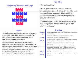
Contributions of the paper • Global optimization as opposed to local individual performance improvement. • Triple Integration: Synthesis/mapping/retiming • Applicability: Standard cells and FPGA’s • Efficiency: Highly scalable, 100k+ gate circuits in about a minute. • Limited to single clock domain and D FF’s, scope for extension.
A quick review of terms • Boolean n/w -> DAG with nodes = gates, edges = wires • AIG -> Only 2 I/P AND gates and inverters • Node, fanin, fanout, Primary I/O’s, transitive fanin & fanout, level of node. • If circuit is sequential, then memory elements are D FF’s with initial states. • Load independent delay model for standard cells.
A quick review of terms • A cut C of node n is a set of nodes of the network, called leaves, such that each path from a PI to n passes through at least one leaf. A trivial cut of the node is the cut composed of the node itself. A cut is K-feasible if it has K leaves or less. • The area and delay of an FPGA mapping is measured by the number of LUTs and the number of LUT levels respectively. • The delay of a standard cell mapping is computed using pin-to-pin delays of gates assigned to implement a cut. • The load-independent timing model is assumed throughout the paper.
Tech mapping is the core procedure in this triple integration!! (Steps) • Prepare the ckt for mapping, by deriving a balanced AIG (use transforms, a(bc) = (ab)c. • Compute K-feasible cuts. • Compute Boolean functions of the cuts. • Match the cuts with LUTS( FPGAs) or gates • Assign delay optimal matches at each node. • Look for the best area match and choose the final mapping in reverse topological order
Combining mapping with retiming • For sequential ckts, use the same concepts as Combinational circuits, except that you consider registers as labels(weights) on the edges. • DAG is now a cyclic circuit(sequential mapping) • So, arrival time measures have to account for labels • Computation of arrival times has to be done by iterating over the circuit. • Resulting mapping has retiming associated with it.
Combining mapping with synthesis • Derive and store MULTIPLE logic structures for the circuit, and finally choose the best one from them. Why ? • Tech independent mapping is heuristic, may produce a sub-optimal network for the given library. A better match may have been discarded earlier. • Synthesis operations apply to the network as a whole. You might want to combine a delay optimized n/w with an area optimized n/w to get the best of both worlds. • However, also note that More choices => more decisions due to more matches at each node!!!!
Constructing the choice network from functionally equivalent, structurally different networks.
Generating choices • Use associativity of the AND operation to locally rewrite the graph. x1(x2x3) = (x1x2)x3 = (x1x3)x2 • Repeat this process until no new AND nodes are created, and thus accumulate choices by applying this sequence of transformations • Choose best combination of choices by using mapping/retiming. This is the final result, obtained by the triple integration method.
High level view of integration flow • FRAIG manager generates choice network from equivalent n/w’s. • Ф = clock period
Experimental results • Experiments on IWLS 2005 benchmarks. • IWLS -> International Workshop on Logic and Synthesis. • Average reduction of clock period is.. • 25% when compared to traditional mapping without retiming. • 20% when compared to traditional mapping with retiming as a post processing step.
Sequential arrival times • Sequential delay of a (possibly) cyclic path p • l(p) = ∑d(n) - Ф ∑t(e) where n,e are in path p. • d(n) : delay of node n. • t(e) : number of registers on edge e. • l(n) = max l(p), considering all paths from PI to n • Ф is infeasible if the arrival time at PO exceeds Ф at any time during the iterative computation.
Retiming associated with final mapping • When optimum clock period Фopt is known( from previous steps), for each node n included in the final mapping, retiming is done using the formula given below, lopt(n) is the sequential arrival time of node n, for Фopt. When this is done, resulting Ф is slower than Фopt by the delay of one gate, at most.