Download
1 / 22
230 likes | 384 Views
Developments on 3D detectors at FBK-irst. Maurizio Boscardin 1 , Luciano Bosisio 3 , Gian-Franco Dalla Betta 2 , Claudio Piemonte 1 , Sabina Ronchin 1 , Andrea Zoboli 2 , Nicola Zorzi 2 1 FBK – IRST, Trento, Italy 2 INFN and University of Trento, Trento, Italy

E N D
Developments on3D detectors at FBK-irst Maurizio Boscardin1, Luciano Bosisio3 , Gian-Franco Dalla Betta2, Claudio Piemonte1, Sabina Ronchin1, Andrea Zoboli2, Nicola Zorzi2 1FBK – IRST, Trento, Italy 2INFN and University of Trento, Trento, Italy 3INFN and University of Trieste, Trieste, Italy 3rd Workshop on Advanced Silicon Radiation Detectors
outline • tecnological strategy • first 3D - DDTC batch • Layout • Electrical characterization • Next Steps (with in-house DRIE) 3rd Workshop on Advanced Silicon Radiation Detectors
Introduction FBK is developing the technology for the production of 3D detectors in a three phases program: 1. First device produced:3D-Single Type Columns “simple” fabrication process, high yield; collection mechanism not very efficient. 2. Performance enhancement with acceptable process complication: 3D-Double Type Columns 3. Full 3D detectors. 3rd Workshop on Advanced Silicon Radiation Detectors
3D DDTC: process and wafer layout Double sided process P-type columns on n-type substrate no hole filling Planar test structures 3D diodes: single and double columns 30 strip detectors, cell size 1cmx1cm, biased by Punch–through structure with AC and DC pads ALICE (5 detectors) MEDIPIX (3 detectors) pixel pixels strip detectors 3D diodes test stuctures 3rd Workshop on Advanced Silicon Radiation Detectors
ALICE pixel detectors 5 devices/wafer (3 with metal on backside) p-type columns 3rd Workshop on Advanced Silicon Radiation Detectors
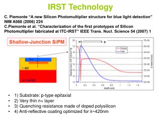
1/C2 Full depletion voltage Planar test structures Diode area: 4mm2 Very low depletion voltage (10V) for 300mm thickness From 1/C2 a substrate concentration of 1.4x 1011 cm-3 Very low leakage current good process Tox = (570-600) nm Qox = (3.6 – 5)x1011 cm-2 from CV on MOS structures So = 1 cm/s from gated diode measurements MOS area: 3.14mm2 Gated diode MOS area: ~1mm2 I/V 3rd Workshop on Advanced Silicon Radiation Detectors
3D-stc & dtc diodes 48 STC & 48 DDTC diodes Active area 16mm x 16mm Either with a uniform (2) or strip like (1) surface implant. Pitch80 have 20 x 20 = 400 columns Pitch100 have 16 x16 = 256 columns 3rd Workshop on Advanced Silicon Radiation Detectors
3D-stc diodes STC diodes exhibit low dark current in agreement with previous batches Less than 0.1pA/col Lateral depletion < 0.5V , full depletion < 3V STC diodes, both 100um and 80 um pitch have the same capacitance value at full depletion (does not depend on pitch) C-V STC diodes Diodes 3rd Workshop on Advanced Silicon Radiation Detectors
Diodi 3D stc – CV From 1/C2 the estimated junction column depth is 190um (not optimized, as expected) Wafers thickness 300um Depleted region under 3D-stc diodes is about ~ 110 - 125um 30-50pA (~2.56mm2; 16x16 or 20x20 colums) 3rd Workshop on Advanced Silicon Radiation Detectors
3D-ddtc diodes I-V measurements Guard Ring Currents Diode Currents • Some DDTC diodes exhibit low dark current similarly to STC ones • Some DDTC diodes show early “breakdown” (current raise) already at low voltage • This effect is present both on main diode and guard ring, but more frequently on the diode. • This suggests a dependence on the number of columns (diode = 256, guard-ring =144) 3rd Workshop on Advanced Silicon Radiation Detectors
3D & planar diodes “breakdown” distribution • Planar Diode ( single guard ring) show a VBK ~ 400V • DTC diodes show early “breakdown” in comparison with STC 3rd Workshop on Advanced Silicon Radiation Detectors
3D-ddtc diodes, C-V 80um 100um Lateral depletion occurs already at built-in voltage. Full depletion at 2V. DTC 80 capacitance saturates before DTC 100 because of the shorter electrode distance. C3D_80um (400cols) = 7pF C3D_100um (256 cols) = 4.8pF 18 fF/column STC DTC 100 DTC 80 3rd Workshop on Advanced Silicon Radiation Detectors
C-V on DDTC test structures (1 col.) The C-V on 1-column diodes gives: C80 = 20 fF C100= 18 fF In good agreements with previous C-V measurements on large diodes. 80 um 100 um C-V simulation A Simulations made with different h coefficient In order to find the value of the ohmic column depth. The structure that fit measurements has ohmic column penetrating 160um into the substrate (not optimized, worse than expected) Because B contribution is dominant, a rough capacitance calculation with the following formula has also been performed : and fits measures with h= (50 ÷ 60 )um 160-170um back column etching B 190um h W C 3rd Workshop on Advanced Silicon Radiation Detectors
AC pads Bias ring guard ring DC pad Strip detectors For each detector: horizontal pitch= vertical pitch number of columns = number of strips Square detectors Cell size = (1x1)cm2 All strips biased by punch-through columns (strips) Radius (um) Surf. implant type pitch readout 30um radius surface implant (other surface geometries available) 3rd Workshop on Advanced Silicon Radiation Detectors
3D-sdtc and ddtc detectors I-V measurements Measurements performed on one wafer 30 strip square detectors Cell size = 1x1cm2 total IV and DC scan @ 5V, 10V, 50V Results STC show a good characteristic DTC detectors exhibit an early “breakdown “. We need to investigate on forthcoming wafers if the problem is still present BUT: “Breakdown” starts between 10V and 20V Full depletion@2V detectors are fully working in the low voltage range. dtc80 stc80 dtc100 stc100 3rd Workshop on Advanced Silicon Radiation Detectors
3D-sdtc detectors I-V measurements D16 3rd Workshop on Advanced Silicon Radiation Detectors
3D-ddtc detectors I-V measurements D13 3rd Workshop on Advanced Silicon Radiation Detectors
Deep-RIE equipment • D-RIE Adixen AMS200 • Preliminary tests made for passing-through etching • Available for processing 3rd Workshop on Advanced Silicon Radiation Detectors
Next batch: n-on-p devices • Few wafers of n-on-p detectors made with external DRIE under way • New batch with in-house DRIE due by end of july 3rd Workshop on Advanced Silicon Radiation Detectors
3D – DDTC2: ATLAS pixel detectors double tc version 200µm-pitch 2 columns/pixel 50µm-pitch 7 columns/pixel 133µm-pitch 3 columns/pixel single tc version 100µm-pitch 4 columns/pixel 3rd Workshop on Advanced Silicon Radiation Detectors
Conclusions • First batch of DDTC has been finally realized! • Detectors feature columns of both doping types, but the process (column depth) is not optimized. • Test structures and detectors were electrically tested, automatic testing (scans) on strip detectors to be completed. • STC are perfect, DTC show early breakdown (with probability proportional to the area defects). • In spite of the non optimized column depth, simulations show a large improvement in the collection time with respect to STC. Functional measurements are under way. • In-house DRIE equipment now available • 3D-DDTC on p-type substrates (including ATLAS pixel layout) should be completed by the end of july 3rd Workshop on Advanced Silicon Radiation Detectors