Download
1 / 25
270 likes | 521 Views
Displacement damage studies of power LDMOS devices for DC-DC conversion. S. Díez , M. Ullán, P. Fernández-Martínez, I. Cortés, S. Hidalgo, D. Flores, G. Pellegrini, M. Lozano, R. Sorge, D. Knoll. Outline. Motivation LDMOS devices from IHP SGB25V GOD technology Neutron irradiations

E N D
Displacement damage studies of power LDMOS devices for DC-DC conversion S. Díez, M. Ullán, P. Fernández-Martínez, I. Cortés, S. Hidalgo, D. Flores, G. Pellegrini, M. Lozano, R. Sorge, D. Knoll
Outline • Motivation • LDMOS devices from IHP SGB25V GOD technology • Neutron irradiations • Additional gamma irradiations • Other studies • Conclusions
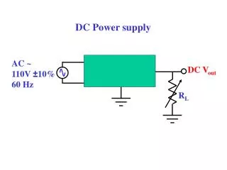
Motivation • DC-DC powering for strips • Laterally Diffused MOS (LDMOS) devices constitute the power switches in buck converters: • Very high cut-off frequency, low losses (low RON) • Implemented into standard (Bi)CMOS technologies (easier than VMOS) • Radiation tolerance must be investigated • Displacement damage investigated with neutron irradiations (complementary to F. Faccio studies, X-rays, p) Faccio et al., IEEE TNS, 2010
LDMOS devices from IHP • 2nd generation devices from IHP GOD module (Gate Overlapped Drift) • Implemented on 0.25 μm SGB25V SiGe BiCMOS technology from IHP Microelectronics • NLDMOS and PLDMOS devices: • Lch x Wch = 2x (0.6x5) μm2 (drawn) • LDrift = 0.6μm (real) • TOX ~ 5 nm • VBR = 22 (-16) V • fT = 20 (10) GHz • RON = 5 (12) Ω·mm • VT = 0.6 (-0.53) V
Radiation damage mechanisms • Nonionizing radiation damage: • Atomic displacement • Vacancies, interstitials, divacancies, impurity atoms,... • DEFECTS on the silicon crystalline lattice = energy levels in the bandgap • Thermal generation of e/h pairs via midgap levels • Thermal recombination of e/h pairs via midgap levels • Scattering centers for carriers • Others: type inversion, transient capture of carriers,... • “Bulk” effect • Normally of secondary concern for MOS devices • May be important for LDMOS devices due to the drift region
Experiment • Neutron irradiations (atomic displacement damage) • TRIGA nuclear reactor at JSI, Ljubljana • 2x10¹³, 2x10¹⁴, 6x10¹⁴, 1x10¹⁵, 2x10¹⁵, 4x10¹⁵, 5x1015 cm-2 (1 MeV neq) • “Parasitic” Total Ionizing Dose (TID): 100 krad(Si) per every 1014 neq/cm2 • Cd shield to avoid thermal neutrons • 4 devices per type and fluence • Devices with terminals floating during irradiations • Annealing: several measurements at RT + 7 days @ 100oC
Results (neutron irrads) • IDS(VDS) curves @ VGS = 2.5 V • Very small changes up to 1x10¹⁵ neq/cm2
Results (neutron irrads) • Threshold voltage shift: Δ|VT| = |VTf|-|VT0| (@ VD = 50 mV) • Max ~ -50 mV for NLDMOS • Max ~ 70 mV for PLDMOS • Mostly related to TID (1-5 Mrad(Si) for 1x10¹⁵- 5x1015 cm-2) • Oxide charges + interface traps: initial decrease for NLDMOS, monotonic VT increase for PLDMOS
Results (neutron irrads) • On-resistance variation: ΔRON = (RONf -RON0) / RON0(%) • Max ~ 35 % for NLDMOS • Max ~ 300 % for PLDMOS • Main effect of displacement damage • Scattering centers in the drift region • Decrease of carriers mobility => Increase of RON
Results (neutron irrads) • Leakage current density: Ileak/w (@ VGS = 0, VD = 15 V) • Observable increase of Ileak • Max < 0.1 nA/μm both for NLDMOS and PLDMOS • Related to thermal generation of e/h pairs via near-midgap levels induced by atomic displacement
Results (neutron irrads) • Annealing: • 2x10¹⁵, 4x10¹⁵ and 5x10¹⁵ neq/cm2 • Devices with terminals floating (same condition as irradiation) • ~ 41 days @ RT (5 measurements) • + 7 days @ 100oC
Results (neutron irrads) • Annealing: Δ|VT| = |VTf|-|VT0| (@ VD = 50 mV) • Little changes of VT • Expected behavior for ionizing radiation damage • Partial annealing of oxide traps, increase of interface traps • ΔVT less negative for NLDMOS • VT more negative for PLDMOS
Results (neutron irrads) • Annealing: ΔRON= (RONf -RON0) / RON0 (%) • Little changes of RON for NLDMOS, as expected, although visible initial change consistently observed w.r.t. post-irrad measurement • Anomalous evolution of RON for PLDMOS • Related to annealing dynamics of the radiation-induced defects producing scattering centers
Results (neutron irrads) • Annealing: Leakage current ( Ileak/w ) • Decrease of Ileak both for NLDMOS and PLDMOS • Annealing of defects producing e/h generation in the channel region of the device
Additional gamma irradiations • Motivation: Identify and separate ionizing and displacement damage from the neutron irradiations • 60Co source at CIEMAT, Madrid (NAYADE water-well source) • 0.65, 5, 10 Mrad(Si) • Devices with floating terminals (same as neutrons) • 4 devices per type and dose • Annealing: same to neutron irrads
Results (gamma irrads) • Δ|VT| = |VTf|-|VT0| (@ VD = 50 mV) • Max ΔVT ~ + 20 mV for NLDMOS devices • Quantitatively in accordance with ΔVT observed after neutron irrads • “Rebound” not observed: probably interface traps dominant in this case • Max Δ|VT|~+ 60 mV for PLDMOS devices • Same ΔVT shift observed after neutron irrads • VT shifts observed after n irrads are mostly due to parasitic TID
Results (gamma irrads) • ΔRON = (RONf -RON0) / RON0 (%) • Negligible changes of RON for NLDMOS • Little changes of RON (related to ΔVT) for PLDMOS • RON change observed in neutron irrads induced by atomic displacement damage
Results (gamma irrads) • Ileak/w • Negligible changes of Ileak for NLDMOS and PLDMOS • Ileak change observed in neutron irrads induced by atomic displacement damage
Standard MOS devices of IHP SGB25V tec • Several standard MOS devices also present in the irradiation test chip • Very similar channel structure as LDMOS devices • Irradiated at the same neutron fluences, under the same conditions as the LDMOS devices • Very similar degradation of VT as LDMOS devices • Confirms that VT change in LDMOS is due to TID effects in the channel region ΔVT NMOS ΔVT PMOS
Simulations • Technological and electrical simulations of IHP GOD LDMOS devices • Status: • Pre-irrad electrical behavior reproduced (starting point) • Radiation damage mechanisms being implemented at the moment
Conclusions • Nonionizing radiation tolerance of 2nd generation SGB25V GOD LDMOS devices from IHP studied • Degradation of electrical characteristics only observable at fluences equal or higher than 1x10¹⁵ neq/cm2 • NLDMOS & PLDMOS devices exhibit small shifts of VT and Ileak at the highest fluence (5x10¹⁵ neq/cm2) • Moderate increase of RON for NLDMOS devices at 5x10¹⁵ neq/cm2 • RON of PLDMOS devices increases dramatically at 5x10¹⁵ neq/cm2 • On the whole, NLDMOS devices are suitable for its application in the SLHC from the p.o.v. of nonionizing radiation tolerance • PLDMOS devices seem more “troubling”
Future work • Ongoing simulations will help understand PLDMOS behavior and radiation damage mechanisms • Understanding 3rd generation issues in collaboration with IHP and F. Faccio • Study the new LDMOS technology generations from IHP • SEB and SEGR studies
NLDMOS detailed cross-section Mohapatra et al., ESSDERC proc., 2005