Download
1 / 17
170 likes | 323 Views
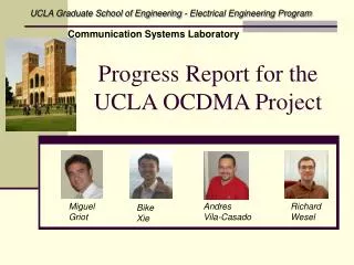
OCDMA Review April 6 th , 2005. Si WDM Modulator Array for FWH-OCDMA. Sagi Mathai, Xin Sun Prof. Tsu-Jae King, Prof. Ming C. Wu EECS Department University of California, Berkeley. FWH-OCDMA All Si Transmitter. Wavelength Selective Microring Modulator Array. Multi-Wavelength Source Input.

E N D
OCDMA Review April 6th, 2005 Si WDM Modulator Arrayfor FWH-OCDMA Sagi Mathai, Xin SunProf. Tsu-Jae King, Prof. Ming C. Wu EECS DepartmentUniversity of California, Berkeley
FWH-OCDMA All Si Transmitter Wavelength Selective Microring Modulator Array Multi-Wavelength Source Input Encoded Output Drop Ports for Feedback Control
Free-Carrier Plasma Effect Absorption Coefficient Change Refractive Index Change Holes Holes -n (cm-1) Electrons Electrons Carrier Concentration (cm-3) Carrier Concentration (cm-3) Ref: Irace, et.al., Silicon Photonics, Topics in Appl Phys, vol 94, pp 361-392, 2004.
Modulation Mechanism SCHEMATIC (TOP VIEW) OPTICAL FREQUENCY RESPONSE si st Modulated Output |st/si|2 n0 n=0 0 sd • Index of refraction can be tuned by injecting or depleting carriers in the microring optical waveguide • Shifting the index of refraction will shift the microring resonant frequency and thus its transfer curve • The resulting modulation in resonant frequency will cause intensity modulation on the optical carrier
Wavelength Channel Distribution FREE SPECTRAL RANGE 4 WAVELENGTH CHANNELS 100 GHz FSR (GHz) FSR = 500 GHz Radius (µm) FSR = 500 GHz corresponds to R = 24 µm
Quality Factor and RC Parasitic Limits QUALITY FACTOR LIMITED BANDWIDTH RC LIMITED BANDWIDTH f3dB (GHz) f3dB (GHz) 0=1.55 µm RL=50 Quality Factor Radius (µm) RC Parasitics do not limited the bandwidth 2.5 Gb/s switching speed requires Q = 80,000 10 Gh/s switching speed requires Q = 20,000
Transfer Function at Resonance POWER TRANSMISSION si st 2 = 0.063 = 0.54 cm-1 sd Carrier Density (cm-3) Target 10 dB Extinction Ratio
Carrier Transport Simulation SWITCHING DYNAMICS CARRIER CONCENTRATION
Previous Results on Passive Si Microdisk Resonators • Microdisk resonators have been fabricated on Si • Optical performance characterized • Optical Q > 100,000 was demonstrated
Si Microring Modulator Schematic P-type Regions Input Port Drop Port Transmit Port SOI N-type Region Add Port
N-type Doping P-type Doping 0.45 m 0.2 m A B 0.05 m 0.45 m BOX Cross Section TOP VIEW C D B A A-B CROSS SECTION C-D CROSS SECTION P-type Doping N-type Doping C D BOX
BPM Waveguide Simulations STRAIGHT WAVEGUIDE CURVED WAVEGUIDE Oxide Oxide Si Si Oxide Oxide Width = 0.45 m Rib height = 0.2 m Slab height = 0.05 m Radius = 24 m
Mask Layout RF and DC Biasing Pads Input Port Transmit Port Microring Resonator 250 microns Drop Port Add Port
Fabrication Process (1) Waveguide Dry Etching (2) Hydrogen Anneal (3) P+ Implant (5) Recrystallization/Dopant Activation Anneal (4) N+ Implant (6) Ni-Silicide (7) Passivation/Via (7) Contact Pads/Interconnect
Complete 0.35μm CMOS on 6” wafers 0.35μm Deep UV Lithography: ASML 5500/90 Stepper Device group demonstrated FIN FET with 60 nm gate length (King, Hu, Bokor) Berkeley Microlab Capability
Si-Modulator Testbed RF Source DC Voltage Source Bias-T DUT IR Camera PC ECTL EDFA VOA /2 Plate Polarizer Free-Space Optical Bench ESA OSA RF Amp BERT PD Oscilloscope Electrical Characterization
Summary • Reviewed preliminary study on an all Si based microring modulator array • Exploit SOI technology and CMOS compatible fabrication process • Built testbed for device characterization • 1st generation device target • 2.5 Gb/s • Single wavelength channel • Free spectral range ~ 0.5 THz • Next generation device • 10 Gb/s • Q = 20,000 • 4 wavelength channels (100 GHz spacing) • Low power (~µW)