Download

1 / 70
700 likes | 773 Views
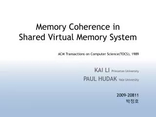
Fundamental Concepts. The Memory System. Some basic concepts. Maximum size of the Main Memory byte-addressable CPU-Main Memory Connection. Memory. Processor. k. -bit. address bus. MAR. n. -bit. data bus. k. Up to 2. addressable. MDR. locations. Word length =. n. bits.

E N D
Fundamental Concepts The Memory System
Some basic concepts • Maximum size of the Main Memory • byte-addressable • CPU-Main Memory Connection Memory Processor k -bit address bus MAR n -bit data bus k Up to 2 addressable MDR locations Word length = n bits Control lines R / W ( , MFC, etc.)
Some basic concepts(Contd.,) • Measures for the speed of a memory: • memory access time - time that elapses b/w the initiation of an operation and the completion of an operation. Eg, time b/w read and MFC s/ls. • memory cycle time– the min time delay b/w the initiation of 2 successive read operations. Its slightly longer than access time. • An important design issue is to provide a computer system with as large and fast a memory as possible, within a given cost target. • Several techniques to increase the effective size and speed of the memory: • Cache memory (to increase the effective speed). • Virtual memory (to increase the effective size).
Semiconductor RAM memories The Memory System
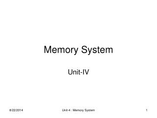
Internal organization of memory chips • Each memory cell can hold one bit of information. • Memory cells are organized in the form of an array. • One row is one memory word. • All cells of a row are connected to a common line, known as the “word line”. • Word line is connected to the address decoder. • Sense/write circuits are connected to the data input/output lines of the memory chip.
Internal organization of memory chips (16x8 organization) b7 b’7 b1 b’1 b b’0 • • • W 0 FF FF A • • • 0 W 1 A 1 Address Memory • • • • • • • • • • • • • • • • • • cells decoder A 2 A 3 • • • W 15 R / W Sense / Write Sense / Write Sense / Write circuit circuit circuit CS Data input /output lines: b b b 7 1 0
To calculate the number of external connections for • address, data & control lines: • For 16x8 organization, • Gnd+Vcc+No of Address pins+Datapins+Control pins • = 1+1+4+8+2 = 16 external connections. • 2. 1K (1024) memory using 128x8 memory needs, • 1+1+7+8+2 = 19 external connections. • 3. 4M using 512Kx8 memory organization needs, • ________ extl.connections.
STATIC memories Memories that consist of circuits capable of retaining their state as long as the power is applied are known as static memories.
SRAM Cell • Two transistor inverters are cross connected to implement a basic flip-flop. • The cell is connected to one word line and two bits lines by transistors T1 and T2 • When word line is at ground level, the transistors are turned off and the latch retains its state • Read operation: In order to read state of SRAM cell, the word line is activated to close switches T1 and T2. Sense/Write circuits at the bottom monitor the state of b and b’ ¢ b b T T 1 2 X Y Word line Bit lines
Static RAMs (SRAMs): • Consist of circuits that are capable of retaining their state as long as the power is applied. • Volatile memories, because their contents are lost when power is interrupted. • Access times of static RAMs are in the range of few nanoseconds. • However, the cost is usually high. • Dynamic RAMs (DRAMs): • Do not retain their state indefinitely. • Contents must be periodically refreshed. • Contents may be refreshed while accessing them for reading.
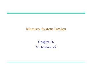
Static memories (2Mx32 memory using 512Kx8 static memory chips) Implement a memory unit of 2M words of 32 bits each. Use 512x8 static memory chips. Each column consists of 4 chips. Each chip implements one byte position. A chip is selected by setting its chip select control line to 1. Selected chip places its data on the data output line, outputs of other chips are in high impedance state. 21 bits to address a 32-bit word. High order 2 bits are needed to select the row, by activating the four Chip Select signals. 19 bits are used to access specific byte locations inside the selected chip. 21-bit 19-bit internal chip address addresses A 0 A 1 A 19 A 20 2-bit decoder 512 K ´ 8 memory chip D D D D 31-24 23-16 15-8 7-0 512 K ´ 8 memory chip 19-bit 8-bit data address input/output Chip select
Dynamic memories • Large dynamic memory systems can be implemented using DRAM chips in a similar way to static memory systems. • Placing large memory systems directly on the motherboard will occupy a large amount of space. Also, this arrangement is inflexible since the memory system cannot be expanded easily. • Packaging considerations have led to the development of larger memory units known as SIMMs (Single In-line Memory Modules) and DIMMs (Dual In-line Memory Modules). • Memory modules are an assembly of memory chips on a small board that plugs vertically onto a single socket on the motherboard. • Occupy less space on the motherboard. • Allows for easy expansion by replacement.
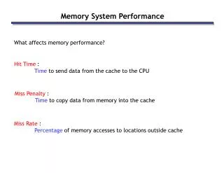
Memory controller • Recall that in a dynamic memory chip, to reduce the number of pins, multiplexed addresses are used. • Address is divided into two parts: • High-order address bits select a row in the array. • They are provided first, and latched using RAS signal. • Low-order address bits select a column in the row. • They are provided later, and latched using CAS signal. • However, a processor issues all address bits at the same time. • In order to achieve the multiplexing, memory controller circuit is inserted between the processor and memory.
Memory controller (contd..) Row/Column address Address R A S R / W C A S Memory controller Request R / W Processor Memory C S Clock Clock Data
Read-Only Memories (ROMs) The Memory System
Read-Only Memories (ROMs) • SRAM and SDRAM chips are volatile: • Lose the contents when the power is turned off. • Many applications need memory devices to retain contents after the power is turned off. • For example, computer is turned on, the operating system must be loaded from the disk into the memory. • Store instructions which would load the OS from the disk. • Need to store these instructions so that they will not be lost after the power is turned off. • We need to store the instructions into a non-volatile memory. • Non-volatile memory is read in the same manner as volatile memory. • Separate writing process is needed to place information in this memory. • Normal operation involves only reading of data, this type of memory is called Read-Only memory (ROM).
Read-Only Memories (Contd.,) • Read-Only Memory: • Data are written into a ROM when it is manufactured. • Programmable Read-Only Memory (PROM): • Allow the data to be loaded by a user. • Process of inserting the data is irreversible. • Storing information specific to a user in a ROM is expensive. • Providing programming capability to a user may be better. • Erasable Programmable Read-Only Memory (EPROM): • Stored data to be erased and new data to be loaded. • Flexibility, useful during the development phase of digital systems. • Erasable, reprogrammable ROM. • Erasure requires exposing the ROM to UV light.
Read-Only Memories (Contd.,) • Electrically Erasable Programmable Read-Only Memory (EEPROM): • To erase the contents of EPROMs, they have to be exposed to ultraviolet light. • Physically removed from the circuit. • EEPROMs the contents can be stored and erased electrically. • Flash memory: • Has similar approach to EEPROM. • Read the contents of a single cell, but write the contents of an entire block of cells. • Flash devices have greater density. • Higher capacity and low storage cost per bit. • Power consumption of flash memory is very low, making it attractive for use in equipment that is battery-driven. • Single flash chips are not sufficiently large, so larger memory modules are implemented using flash cards and flash drives.
Speed, Size, and Cost • A big challenge in the design of a computer system is to provide a sufficiently large memory, with a reasonable speed at an affordable cost. • Static RAM: • Very fast, but expensive, because a basic SRAM cell has a complex circuit making it impossible to pack a large number of cells onto a single chip. • Dynamic RAM: • Simpler basic cell circuit, hence are much less expensive, but significantly slower than SRAMs. • Magnetic disks: • Storage provided by DRAMs is higher than SRAMs, but is still less than what is necessary. • Secondary storage such as magnetic disks provide a large amount of storage, but is much slower than DRAMs.
Fastest access is to the data held in • processor registers. Registers are at • the top of the memory hierarchy. • Relatively small amount of memory that • can be implemented on the processor • chip. This is processor cache. • Two levels of cache. Level 1 (L1) cache • is on the processor chip. Level 2 (L2) • cache is in between main memory and • processor. • Next level is main memory, implemented • as SIMMs. Much larger, but much slower • than cache memory. • Next level is magnetic disks. Huge amount • of inexepensive storage. • Speed of memory access is critical, the • idea is to bring instructions and data • that will be used in the near future as • close to the processor as possible. Pr ocessor Re gisters Increasing Increasing Increasing size speed cost per bit Primary L1 cache Secondary L2 cache Main memory Magnetic disk secondary memory Memory Hierarchy
Cache Memories The Memory System
Cache Memories • Processor is much faster than the main memory. • As a result, the processor has to spend much of its time waiting while instructions and data are being fetched from the main memory. • Major obstacle towards achieving good performance. • Speed of the main memory cannot be increased beyond a certain point. • Cache memory is an architectural arrangement which makes the main memory appear faster to the processor than it really is. • Cache memory is based on the property of computer programs known as “locality of reference”.
Locality of Reference • Analysis of programs indicates that many instructions in localized areas of a program are executed repeatedly during some period of time, while the others are accessed relatively less frequently. • These instructions may be the ones in a loop, nested loop or few procedures calling each other repeatedly. • This is called “locality of reference”. • Temporal locality of reference: • Recently executed instruction is likely to be executed again very soon. • Spatial locality of reference: • Instructions with addresses close to a recently instruction are likely to be executed soon.
Cache memories • Processor issues a Read request, a block of words is transferred from the main memory to the cache, one word at a time. • Subsequent references to the data in this block of words are found in the cache. • At any given time, only some blocks in the main memory are held in the cache. Which blocks in the main memory are in the cache is determined by a “mapping function”. • When the cache is full, and a block of words needs to be transferred from the main memory, some block of words in the cache must be replaced. This is determined by a “replacement algorithm”. Main Processor Cache memory
Cache hit • Existence of a cache is transparent to the processor. The processor issues Read and Write requests in the same manner. • If the data is in the cache it is called a Read or Write hit. • Read hit: • The data is obtained from the cache. • Write hit: • Cache has a replica of the contents of the main memory. • Contents of the cache and the main memory may be updated simultaneously. This is the write-through protocol. • Update the contents of the cache, and mark it as updated by setting a bit known as the dirty bit or modified bit. The contents of the main memory are updated when this block is replaced. This is write-back or copy-back protocol.
Cache miss • If the data is not present in the cache, then a Read miss or Write miss occurs. • Read miss: • Block of words containing this requested word is transferred from the memory. • After the block is transferred, the desired word is forwarded to the processor. • The desired word may also be forwarded to the processor as soon as it is transferred without waiting for the entire block to be transferred. This is called load-through or early-restart. • Write-miss: • Write-through protocol is used, then the contents of the main memory are updated directly. • If write-back protocol is used, the block containing the addressed word is first brought into the cache. The desired word is overwritten with new information.
Mapping functions • Mapping functions determine how memory blocks are placed in the cache. • A simple processor example: • Cache consisting of 128 blocks of 16 words each. • Total size of cache is 2048 (2K) words. • Main memory is addressable by a 16-bit address. • Main memory has 64K words. • Main memory has 4K blocks of 16 words each. • Three mapping functions: • Direct mapping • Associative mapping • Set-associative mapping.
Main memory T ag Block W ord 5 7 4 Main memory address Direct mapping • Block j of the main memory maps to j modulo 128 of • the cache. 0 maps to 0, 129 maps to 1. • More than one memory block is mapped onto the same • position in the cache. • May lead to contention for cache blocks even if the • cache is not full. • Resolve the contention by allowing new block to • replace the old block, leading to a trivial replacement • algorithm. • Memory address is divided into three fields: • - Low order 4 bits determine one of the 16 • words in a block. • - When a new block is brought into the cache, • the the next 7 bits determine which cache • block this new block is placed in. • - High order 5 bits determine which of the possible • 32 blocks is currently present in the cache. These • are tag bits. • Simple to implement but not very flexible. Block 0 Block 1 Cache tag Block 0 tag Block 1 Block 127 Block 128 tag Block 129 Block 127 Block 255 Block 256 Block257 Block 4095
Main memory Tag Word 12 4 Main memory address Associative mapping Block 0 • Main memory block can be placed into any cache • position. • Memory address is divided into two fields: • - Low order 4 bits identify the word within a block. • - High order 12 bits or tag bits identify a memory • block when it is resident in the cache. • Flexible, and uses cache space efficiently. • Replacement algorithms can be used to replace an • existing block in the cache when the cache is full. • Cost is higher than direct-mapped cache because of • the need to search all 128 patterns to determine • whether a given block is in the cache. Block 1 Cache tag Block 0 tag Block 1 Block 127 Block 128 tag Block 129 Block 127 Block 255 Block 256 Block 257 Block 4095
Main memory T ag Block W ord 5 7 4 Main memory address Set-Associative mapping Cache Blocks of cache are grouped into sets. Mapping function allows a block of the main memory to reside in any block of a specific set. Divide the cache into 64 sets, with two blocks per set. Memory block 0, 64, 128 etc. map to block 0, and they can occupy either of the two positions. Memory address is divided into three fields: - 6 bit field determines the set number. - High order 6 bit fields are compared to the tag fields of the two blocks in a set. Set-associative mapping combination of direct and associative mapping. Number of blocks per set is a design parameter. - One extreme is to have all the blocks in one set, requiring no set bits (fully associative mapping). - Other extreme is to have one block per set, is the same as direct mapping. Block 0 tag Block 1 tag Block 1 Block 2 tag tag Block 3 Block 0 Block 63 Block 64 tag Block 65 Block 126 tag Block 127 Block 127 Block 128 Block129 Block 4095
Performance considerations The Memory System
Performance considerations • A key design objective of a computer system is to achieve the best possible performance at the lowest possible cost. • Price/performance ratio is a common measure of success. • Performance of a processor depends on: • How fast machine instructions can be brought into the processor for execution. • How fast the instructions can be executed.
Interleaving • Divides the memory system into a number of memory modules. Each module has its own address buffer register (ABR) and data buffer register (DBR). • Arranges addressing so that successive words in the address space are placed in different modules. • When requests for memory access involve consecutive addresses, the access will be to different modules. • Since parallel access to these modules is possible, the average rate of fetching words from the Main Memory can be increased.
Methods of address layouts m bits k bits k bits m bits Address in module Module MM address • Consecutive words are placed in a module. • High-order k bits of a memory address determine the module. • Low-order m bits of a memory address determine the word within a module. • When a block of words is transferred from main memory to cache, only one module is busy at a time. Module Address in module MM address ABR DBR ABR DBR ABR DBR ABR DBR ABR DBR ABR DBR Module Module Module k 2 - 1 0 i Module Module Module n - 1 0 i • Consecutive words are located in consecutive modules. • Consecutive addresses can be located in consecutive modules. • While transferring a block of data, several memory modules can be kept busy at the same time.
Hit Rate and Miss Penalty • Hit rate: The no of hits stated as a fraction of all attempted accesses. • Miss rate: The no of misses stated as a fraction of attempted accesses. • Miss penalty: The extra time needed to bring the desired information into the cache • Hit rate can be improved by increasing block size, while keeping cache size constant • Miss penalty can be reduced if load-through approach is used when loading new blocks into cache.
Caches on the processor chip • In high performance processors 2 levels of caches are normally used. • Avg access time in a system with 2 levels of caches is T ave = h1c1+(1-h1)h2c2+(1-h1)(1-h2)M Where h1 = hit rate in L1 cache, h2=hit rate in L2 cache, C1=time to access information in L1 cache, C2=time to access information in L2 cache, M= time to access information in main memory.
Other Performance Enhancements Write buffer • Write-through: • Each write operation involves writing to the main memory. • If the processor has to wait for the write operation to be complete, it slows down the processor. • Processor does not depend on the results of the write operation. • Write buffer can be included for temporary storage of write requests. • Processor places each write request into the buffer and continues execution. • If a subsequent Read request references data which is still in the write buffer, then this data is referenced in the write buffer. • Write-back: • Block is written back to the main memory when it is replaced. • If the processor waits for this write to complete, before reading the new block, it is slowed down. • Fast write buffer can hold the block to be written, and the new block can be read first.
Other Performance Enhancements (Contd.,) Prefetching • New data are brought into the processor when they are first needed. • Processor has to wait before the data transfer is complete. • Prefetch the data into the cache before they are actually needed, or a before a Read miss occurs. • Prefetching can be accomplished through software by including a special instruction in the machine language of the processor. • Inclusion of prefetch instructions increases the length of the programs. • Prefetching can also be accomplished using hardware: • Circuitry that attempts to discover patterns in memory references and then prefetches according to this pattern.
Other Performance Enhancements (Contd.,) Lockup-Free Cache • Prefetching scheme does not work if it stops other accesses to the cache until the prefetch is completed. • A cache of this type is said to be “locked” while it services a miss. • Cache structure which supports multiple outstanding misses is called a lockup free cache. • Since only one miss can be serviced at a time, a lockup free cache must include circuits that keep track of all the outstanding misses. • Special registers may hold the necessary information about these misses.
Virtual Memory The Memory System
Virtual memories • Recall that an important challenge in the design of a computer system is to provide a large, fast memory system at an affordable cost. • Architectural solutions to increase the effective speed and size of the memory system. • Cache memories were developed to increase the effective speed of the memory system. • Virtual memory is an architectural solution to increase the effective size of the memory system.
Virtual memories (contd..) • Recall that the addressable memory space depends on the number of address bits in a computer. • For example, if a computer issues 32-bit addresses, the addressable memory space is 4G bytes. • Physical main memory in a computer is generally not as large as the entire possible addressable space. • Physical memory typically ranges from a few hundred megabytes to 1G bytes. • Large programs that cannot fit completely into the main memory have their parts stored on secondary storage devices such as magnetic disks. • Pieces of programs must be transferred to the main memory from secondary storage before they can be executed.
Virtual memories (contd..) • When a new piece of a program is to be transferred to the main memory, and the main memory is full, then some other piece in the main memory must be replaced. • Recall this is very similar to what we studied in case of cache memories. • Operating system automatically transfers data between the main memory and secondary storage. • Application programmer need not be concerned with this transfer. • Also, application programmer does not need to be aware of the limitations imposed by the available physical memory.
Virtual memories (contd..) • Techniques that automatically move program and data between main memory and secondary storage when they are required for execution are called virtual-memory techniques. • Programs and processors reference an instruction or data independent of the size of the main memory. • Processor issues binary addresses for instructions and data. • These binary addresses are called logical or virtual addresses. • Virtual addresses are translated into physical addresses by a combination of hardware and software subsystems. • If virtual address refers to a part of the program that is currently in the main memory, it is accessed immediately. • If the address refers to a part of the program that is not currently in the main memory, it is first transferred to the main memory before it can be used.
Virtual memory organization Processor • Memory management unit (MMU) translates • virtual addresses into physical addresses. • If the desired data or instructions are in the • main memory they are fetched as described • previously. • If the desired data or instructions are not in • the main memory, they must be transferred • from secondary storage to the main memory. • MMU causes the operating system to bring • the data from the secondary storage into the • main memory. Virtual address Data MMU Physical address Cache Data Physical address Main memory DMA transfer Disk storage
Address translation • Assume that program and data are composed of fixed-length units called pages. • A page consists of a block of words that occupy contiguous locations in the main memory. • Page is a basic unit of information that is transferred between secondary storage and main memory. • Size of a page commonly ranges from 2K to 16K bytes. • Pages should not be too small, because the access time of a secondary storage device is much larger than the main memory. • Pages should not be too large, else a large portion of the page may not be used, and it will occupy valuable space in the main memory.
Address translation (contd..) • Concepts of virtual memory are similar to the concepts of cache memory. • Cache memory: • Introduced to bridge the speed gap between the processor and the main memory. • Implemented in hardware. • Virtual memory: • Introduced to bridge the speed gap between the main memory and secondary storage. • Implemented in part by software.
Address translation (contd..) • Each virtual or logical address generated by a processor is interpreted as a virtual page number (high-order bits) plus an offset (low-order bits) that specifies the location of a particular byte within that page. • Information about the main memory location of each page is kept in the page table. • Main memory address where the page is stored. • Current status of the page. • Area of the main memory that can hold a page is called as page frame. • Starting address of the page table is kept in a page table base register.
Address translation (contd..) • Virtual page number generated by the processor is added to the contents of the page table base register. • This provides the address of the corresponding entry in the page table. • The contents of this location in the page table give the starting address of the page if the page is currently in the main memory.
Address translation (contd..) PTBR holds the address of the page table. Virtual address from processor Page table base register Page table address Virtual page number Offset Virtual address is interpreted as page number and offset. + PAGE TABLE PTBR + virtual page number provide the entry of the page in the page table. This entry has the starting location of the page. Page table holds information about each page. This includes the starting address of the page in the main memory. Control Page frame bits in memory Page frame Offset Physical address in main memory