Memory Sub-System
Memory Sub-System. CT213 – Computing Systems Organization. Memory Subsystem. Memory Hierarchy Types of memory Memory organization Memory Hierarchy Design Cache. Memory Hierarchy. Registers In CPU Internal or Main memory May include one or more levels of cache “RAM” External memory

Memory Sub-System
E N D
Presentation Transcript
Memory Sub-System CT213 – Computing Systems Organization
Memory Subsystem • Memory Hierarchy • Types of memory • Memory organization • Memory Hierarchy Design • Cache
Memory Hierarchy • Registers • In CPU • Internal or Main memory • May include one or more levels of cache • “RAM” • External memory • Backing store
External Memory Types • HDD • Magnetic Disk(s) • SDD (Solid State Disk(s)) • Optical • CD-ROM • CD-Recordable (CD-R) • CD-R/W • DVD • Magnetic Tape
Random Access Memory (RAM) • Misnamed as all semiconductor memory is random access • Read/Write • Volatile • Temporary storage • Static or dynamic
Types of RAM • Dynamic RAM (DRAM) – are like leaky capacitors; initially data is stored in the DRAM chip, charging its memory cells to maximum values. The charge slowly leaks out and eventually would go to low to represent valid data; before this happens, a refresh circuitry reads the contents of the DRAM and rewrites the data to its original locations, thus restoring the memory cells to their maximum charges • Static RAM (SRAM) – is more like a register; once the data has been written, it will stay valid, it doesn’t have to be refreshed. Static RAM is faster than DRAM, also more expensive. Cache memory in PCs is constructed from SRAM memory.
Dynamic RAM • Bits stored as charge in capacitors • Charges leak • Need refreshing even when powered • Simpler construction • Smaller per bit • Less expensive • Need refresh circuits • Slower • Used for main memory in computing systems • Essentially analogue • Level of charge determines value
DRAM Operation • Address line active when bit read or written • Transistor switch closed (current flows) • Write • Voltage to bit line • High for 1 low for 0 • Then signal address line • Transfers charge to capacitor • Read • Address line selected • transistor turns on • Charge from capacitor fed via bit line to sense amplifier • Compares with reference value to determine 0 or 1 • Capacitor charge must be restored
DRAM Refreshing • Refresh circuit included on chip • Disable chip • Count through rows • Read & Write back • Takes time • Slows down apparent performance
Static RAM • Bits stored as on/off switches • No charges to leak • No refreshing needed when powered • More complex construction • Larger per bit • More expensive • Does not need refresh circuits • Faster • Cache • Digital • Uses flip-flops
Static RAM Operation • Transistor arrangement gives stable logic state • State 1 • C1 high, C2 low • T1 T4 off, T2 T3 on • State 0 • C2 high, C1 low • T2 T3 off, T1 T4 on • Address line transistors T5 T6 is switch • Write – apply value to B & compliment to B • Read – value is on line B
SRAM v DRAM • Both volatile • Power needed to preserve data • Dynamic cell • Simpler to build, smaller • More dense • Less expensive • Needs refresh • Larger memory units • Static • Faster • Cache
Read Only Memory (ROM) • Permanent storage • Nonvolatile • Microprogramming • Library subroutines (code) and constant data • Systems programs (BIOS for PC or entire application + OS for certain embedded systems)
Types of ROM • Written during manufacture • Very expensive for small runs • Programmable (once) • PROM • Needs special equipment to program • Read “mostly” • Erasable Programmable (EPROM) • Erased by UV • Electrically Erasable (EEPROM) • Takes much longer to write than read • Flash memory • Erase whole memory electrically
Internal linear organization • 8X2 ROM chip • As the number of locations increases, the size of the address decoder needed, becomes very large • Multiple dimensions of decoding can be used to overcome this problem
Internal two-dimensional organization • High order address bits (A2A1) select one of the rows • The low order address bit selects one of the two locations in the row
Memory Subsystems Organization (1) • Two or more memory chips can be combined to create memory with more bits per location (two 8X2 chips can create a 8X4 memory)
Memory Subsystems Organization (2) • Two or more memory chips can be combined to create more locations (two 8X2 chips can create 16X2 memory)
Memory Hierarchy Design (1) • Since 1987, microprocessors performance improved 55% per year and 35% until 1987 • This picture shows the CPU performance against memory access time improvements over the years • Clearly there is a processor-memory performance gap that computer architects must take care of
Memory Hierarchy Design (2) • It is a tradeoff between size, speed and cost and exploits the principle of locality. • Register • Fastest memory element; but small storage; very expensive • Cache • Fast and small compared to main memory; acts as a buffer between the CPU and main memory: it contains the most recent used memory locations (address and contents are recorded here) • Main memory is the RAM of the system • Disk storage - HDD
Memory Hierarchy Design (3) • Comparison between different types of memory HDD Register Cache Memory size: speed: $/Mbyte: 32 - 256 B 1-2 ns 32KB - 4MB 2-4 ns $20/MB 1000 MB 60 ns $0.2/MB 200 GB 8 ms $0.001/MB larger, slower, cheaper
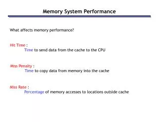
Memory Hierarchy Design (4) • Design questions about any level of the memory hierarchy: • Where can a block be placed in the upper level? • BLOCK PLACEMENT • How is a block found if it is in the upper level? • BLOCK IDENTIFICATION • Which block should be replaced on a miss? • BLOCK REPLACEMENT • What happens on a write? • WRITE STRATEGY
Cache (1) • Is the first level of memory hierarchy encountered once the address leaves the CPU • Since the principle of locality applies, and taking advantage of locality to improve performance is so popular, the term cache is now applied whenever buffering is employed to reuse commonly occurring items • We will study caches by trying to answer the four questions for the first level of the memory hierarchy
Cache (2) • Every address reference goes first to the cache; • if the desired address is not here, then we have a cache miss; • The contents are fetched from main memory into the indicated CPU register and the content is also saved into the cache memory • If the desired data is in the cache, then we have a cache hit • The desired data is brought from the cache, at very high speed (low access time) • Most software exhibits temporal locality of access, meaning that it is likely that same address will be used again soon, and if so, the address will be found in the cache • Transfers between main memory and cache occur at granularity of cache lines or cache blocks, around 32 or 64 bytes (rather than bytes or processor words). Burst transfers of this kind receive hardware support and exploit spatial locality of access to the cache (future access are often to address near to the previous one)
Where can a block be placed in Cache? (1) • Our cache has eight block frames and the main memory has 32 blocks
Where can a block be placed in Cache? (2) • Direct mapped Cache • Each block has only one place where it can appear in the cache • (Block Address) MOD (Number of blocks in cache) • Fully associative Cache • A block can be placed anywhere in the cache • Set associative Cache • A block can be placed in a restricted set of places into the cache • A set is a group of blocks into the cache • (Block Address) MOD (Number of sets in the cache) • If there are n blocks in the cache, the placement is said to be n-way set associative
How is a Block Found in the Cache? • Caches have an address tag on each block frame that gives the block address. The tag is checked against the address coming from CPU • All tags are searched in parallel since speed is critical • Valid bit is appended to every tag to say whether this entry contains valid addresses or not • Address fields: • Block address • Tag – compared against for a hit • Index – selects the set • Block offset – selects the desired data from the block • Set associative cache • Large index means large sets with few blocks per set • With smaller index, the associativity increases • Full associative cache – index field is not existing
Which Block should be Replaced on a Cache Miss? • When a miss occurs, the cache controller must select a block to be replaced with the desired data • Benefit of direct mapping is that the hardware decision is much simplified • Two primary strategies for full and set associative caches • Random – candidate blocks are randomly selected • Some systems generate pseudo random block numbers, to get reproducible behavior useful for debugging • LRU (Least Recently Used) – to reduce the chance that information that has been recently used will be needed again, the block replaced is the least-recently used one. • Accesses to blocks are recorded to be able to implement LRU
What Happens on a Write? • Two basic options when writing to the cache: • Writhe through – the information is written to both, the block in the cache an the block in the lower-level memory • Write back – the information is written only to the cache • The modified block of cache is written back into the lower-level memory only when it is replaced • To reduce the frequency of writing back blocks on replacement, an implementation feature called dirty bit is commonly used. • This bit indicates whether a block is dirty (has been modified since loaded) or clean (not modified). If clean, no write back is involved
Alpha Processors Cache Example 1 – the address comes from the CPU, being divided into 29 bit block address and 5 bit offset. The block address is further divided into 21 bit tag and 8 bit index 2 – the cache index selects the tag to be tested to see if the desired block is in the cache. The size of the index depends on the cache size, block size and the set associativity 3 – after reading the tag from the cache, it is compared with the tag from the address from the CPU. The valid bit must be set, otherwise, the result of comparison is ignored. 4 – assuming the tag does match, the final step is to signal the CPU to load the data from the cache.
References • “Computer Architecture – A Quantitative Approach”, John L Hennessy & David A Patterson, ISBN 1-55860-329-8 • “Computer Systems Organization & Architecture”, John D. Carpinelli, ISBN: 0-201-61253-4 • “Computer Organization and Architecture”, William Stallings, 8th Edition
Detailed Direct Mapping Example • Cache of 64kByte • Cache block of 4 bytes • i.e. cache is 16k (214) lines of 4 bytes • 16MBytes main memory • 24 bit address (224=16M) • Address is in two parts • Least Significant w bits identify unique word • Most Significant s bits specify one memory block • The MSBs are split into a cache line field r and a tag of s-r (most significant)
Direct Mapping Example - Address Structure • 24 bit address • 2 bit word identifier (4 byte block) • 22 bit block identifier • 8 bit tag (=22-14) • 14 bit slot or line • No two blocks in the same line have the same Tag field • Check contents of cache by finding line and checking Tag Tag s-r Line (Index) r Word w 14 2 8
Direct Mapping Cache Organization Mapping function i = j mod m
Detailed Fully Associative Mapping Example • Cache of 64kByte • Cache block of 4 bytes • i.e. cache is 16k (214) lines of 4 bytes • 16MBytes main memory • 24 bit address (224=16M) • A main memory block can load into any line of cache • Memory address is interpreted as tag and word • Tag uniquely identifies block of memory • Every line’s tag is examined for a match • Cache searching gets expensive
Fully Associative Mapping Example - Address Structure • 22 bit tag stored with each 32 bit block of data • Compare tag field with tag entry in cache to check for hit • Least significant 2 bits of address identify which word is required from 32 bit data block • e.g. • Address Tag Data Cache line • FFFFFC FFFFFC 0x24682468 3FFF Word 2 bit Tag 22 bit
Detailed Set Associative Mapping Example • Cache of 64kByte • Cache block of 4 bytes • i.e. cache is 16k (214) lines of 4 bytes • 16MBytes main memory • 24 bit address (224=16M) • Cache is divided into a number of sets (v) • Each set contains a number of lines (k) • A given block maps to any line in a given set • e.g. Block B can be in any line of set i • Mapping function • i = j mod v (where total lines in the cache m = v * k) • J – main memory block • I – cache set number • e.g. 2 lines per set • 2 way associative mapping (k = 2) • A given block can be in one of 2 lines in only one set
Example Set Associative Mapping - Address Structure Word 2 bit Tag 9 bit Set (Index) 13 bit • Use set field to determine cache set to look in • Compare tag field to see if we have a hit • e.g • Address Tag Data Set • 1FF 7FFC 1FF 12345678 1FFF • 001 7FFC 001 11223344 1FFF