GUI MATLAB
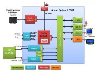
Filter. FLASH Memory On DE2 board. Altera Cyclone II FPGA. CCB_disable. SPANSION S29AL032D. Flash Contro l. Intercon Wishbone. WBS 6. WBS 3. Wait. 4M x 8 bits . WBS 4. LED X 4. ADV7123 Video DAC. 5 WBS . DISPLAY. Clk 100MHz. Config Control. Clk 50MHz. Clk & Reset.

GUI MATLAB
E N D
Presentation Transcript
Filter FLASH Memory On DE2 board Altera Cyclone II FPGA CCB_disable SPANSION S29AL032D Flash Control Intercon Wishbone WBS 6 WBS 3 Wait 4M x 8 bits WBS 4 LED X 4 ADV7123 Video DAC 5WBS DISPLAY Clk 100MHz Config Control Clk 50MHz Clk & Reset Clk 65MHz WBM 3 1024 x 768@60Hz Reset WBS 7 LCD Reset RAM HD44780 UART IN 115200 bits/sec RX PATH WBS 1 WBM 1 GUI MATLAB WBS 2 TX PATH WBM 2 UART OUT 115200 bits/sec Implemented Integrated Next steps Optional
WBM 1 RXPath Message decoder to wishbone master Frame_error Frame_OK type UART RX Message Decoder len error address UART_IN valid Data [7..0] RAM Data [7..0] crc Read_enable Read enable CRC Read_value Read enable
WBS 1 WBM 2 Wishbone to message encoder type TX Path CRC address len Frame _finish crc Frame _OK crc Wishbone_data [7..0] UART_OUT UART TX Wishbone_data [7..0] Message encoder Data package valid busy RAM Write_enable
Clk & Reset Sys_clk[100 MHz] PLL Vesa_clk[65 MHz] CLK [50MHz] Vesa_reset Reset_in lock Reset block Sys_reset
Filter Sig_filtered Sig_in CLK [100MHz] Sys_reset Sig_in Sig_filtered
Sys_clk Sys_reset WBS 4 Ledcontrol Enable X 4 Led X 4 freq_enable X 4 Led registers Freq [7..0] X 4 counter Timer_enable Sys_reset Sys_clk Timer X 4 Timer_tic
Wishbone Slave 5 Display Client Synthetic data provider VESA generator REGS Clock domain crossing 100 MHz 65 MHz
Sys_clk Sys_reset WBS 2 Wait Wait control start Wait_reg finish counter REGS Timer_enable Sys_reset Sys_clk Timer Timer_tic
Message pack structure Type Len Address Data Data Len Data EOD
Transmit=0 Idle transmit= 1 Read regs transmit= 1 wr_en= 1 transmit= 1 wr_en= 0 valid_data_in=0 Wait for RAM data Read ACK_I=0 Valid_data_in=1 Sample RAM data ACK_I=1 transmit= 1 transmit= 1 Transfer data to RAM End read End write ACK_I=1 Write ACK_I=0
Mp_clone=0 Idle Mp_clone= 1 Sample Registers And send To WM Len=0 calculate Len<=len-1 Len=!0 ACK_I=1 Read_ RAM transmit RAM_valid=1 RAM_valid=0 ACK_I=0
RX_path Wishbone master bus Mp_done MDWM errors Uart_in Uart_rx errors Message Pack decoder RAM_read RAM_write RAM CRC Error register Wishbone slave bus errors
Top_level Master 1 Uart_tx Gen_model Slave 3 wait Rx_path Slave 1 Wishbone _intercon LED_activate Slave 4 LED Master 2 Uart_out tx_path Slave 2
FSM Wishbone slave 1 Idle CYC_1 Wishbone Master 1 Wishbone slave 2 M1 CYC_2 M2 M3 Wishbone slave 3 CYC_3 Wishbone Master 2 Master enable Master chooser demax Wishbone Slave 4 to Master Slave signals MUX Wishbone Slave 5 Wishbone Master 3 Wishbone Slave 6 Slave chooser Slave enable demax Wishbone Slave 7 Master signals To slave MUX Wishbone Intercon
Ledcontrol enable Led_activate freq_enable Freq [7..0] counter Timer_enable Timer Timer_tic