Download
1 / 25
270 likes | 486 Views
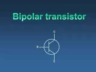
Scalable bipolar transistor modelling with HICUM L0. S. Frégonèse, D. Berger * , T. Zimmer, C. Maneux, P. Y. Sulima, D. Céli * Laboratoire de Microélectronique IXL, FRANCE * ST Microelectronics, FRANCE. Outlines. Introduction Geometry Scaling Modelling strategy Why HICUM L0 ?

E N D
Scalable bipolar transistor modelling with HICUM L0 S. Frégonèse, D. Berger*, T. Zimmer, C. Maneux, P. Y. Sulima, D. Céli* Laboratoire de Microélectronique IXL, FRANCE * ST Microelectronics, FRANCE HICUM WORKSHOP 2004
Outlines • Introduction • Geometry Scaling • Modelling strategy • Why HICUM L0 ? • HICUM L0 & L2 • Similarity between L2 and L0 • L0 equations • Applications • Extraction • Impact of emitter via resistances • Impact of corner rounding • DC & AC measurement and model comparison • Conclusion • Perspectives HICUM WORKSHOP 2004
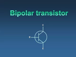
r0 WE0 LE0 gC Mask E B C Introduction : Geometry scaling • Transistor modelling with a function of emitter length and width as parameters • Circuit performances optimisation • Model many transistors with one parameter set • Important parameter for scalable modelling of the internal transistor • Real length and width ( WE0 and LE0 ) • Spacer have to be taken into account • Effective diffusion length under emitter window gC • Corner rounding • Low size transistor • SIC window • Internal & external base collector capacitancesmodelling • Base Collector current HICUM WORKSHOP 2004
Introduction : Modelling Strategy HICUM WORKSHOP 2004
Introduction : Why HICUM L0 ? • A new model combining • Simplicity of Gummel Poon: • Less computational effort (internal nodes number, L0 : 3,L2 : 5) • Extraction is easier • Major features of HICUM • Accurate charge description • Self heating is taken into account • Useful for: • Quick evaluation of the basic circuit functionality • For non critical transistor HICUM WORKSHOP 2004
HICUM L0 & L2 :Similarity between L0 and L2 • Simplifications • Charge: • Simplification of charge modelling in transfer current source • DC and AC are uncorrelated. • Internal base node is suppressed • External base resistance and internal base resistance are merged together • External base-emitter capacitance and internal base-emitter capacitance are grouped together • Current source are merged: • Peripheral and internal base-collector • Peripheral and internal base-emitter • Others effects: • Substrate network • Parasistic transistor • NQS effects • Base-Emitter tunnelling current source HICUM WORKSHOP 2004
HICUM L0 & L2 :Similarity between L0 and L2 • AC Charge formulation unchanged • Capacitance formulation • Transit time formulation • At low & high current • Critical current • Internal base resistance: • Temperature dependence & self heating Geometry dependent zero bias value is unchanged Bias variation function is simplified HICUM WORKSHOP 2004
HICUM L0 & L2 : L0 Equations - Transfert current source in HICUM L0 -Transfer current source in HICUM L2 - Low to medium current : -Low current: - Low current: 1 scalable parameter 1 constant parameter 2 scalable parameters HICUM WORKSHOP 2004
HICUM L0 & L2 : L0 Equations • - Charge increase for DC regime: • AC et DC are uncorrelated - Charge increase for AC regime: Same equation as L2 fcs function parameter is extracted from RCI0 extraction ( from AC characteristics) HICUM WORKSHOP 2004
Applications : Extraction flow Transit time @ low current t0I, t0P, TBVL, DT0H CBE, CBCi, CBCx, CCS Critical current parameters RCI0U, dC,VCES, VPT, VLIM gC and Collector current source (Jcu, mcf) Transit time @ high current tEF0, GTE, tHCS, ALHC base-emitter & base-collector current source RE is extracted / RCX, RBX, RBI are calculated from layer resistivity DC charge @ high current IQFHu, tFH HICUM WORKSHOP 2004
Applications : Extraction of Capacitance • CBE=CBEpuPE0+CBEsuAE0 HICUM WORKSHOP 2004
Collector current versus emitter width for different VBE and VBC=0 V (measurement) r0 WE0 LE0 gC Mask E B C Applications : Extraction of gC • IC=JC(WE0+2gC)(LE0+2gC) • IC=0 if WE0=-2gC HICUM WORKSHOP 2004
Applications: Extraction of Transit time • Split into one internal part and into one peripheral part: • Ic=Ii+Ip= JiAE0+JpPE • Qtotal= Q0i+ Q0P • Internal charge: Q0i=t0iIi • Peripheral charge: Q0P=t0PIP • Equivalent transit time - t0=Qtotal/Ic • Scalable model [1] : • Extracted t0 values versus emitter area for different emitter sizes. (1: 0.25*1.45 µm², 2: 0.25*3.05 µm², 3: 0.25*6.25 µm², 4: 0.25*12.65 µm², 5: 0.25*25.45 µm², 6: 0.65*12.65 µm², 7: 1.45*12.65 µm²) HICUM WORKSHOP 2004 [1] Michael Schröeter et al. IEEE solid states circuits, vol .31, n°10, oct 1996
Applications :Extraction of Critical current parameter • Critical current • Models the transit frequency fall- off • Link to Kirk effect • Collector doping • Internal collector resistance: • Current spreading in the collector with a dC angle • Scalable model [1] fcs Extracted RCI0 values versus emitter area for different emitter sizes. (1: 0.25*1.45 µm², 2: 0.25*3.05 µm², 3: 0.25*6.25 µm², 4: 0.25*12.65 µm², 5: 0.25*25.45 µm², 6: 0.65*12.65 µm², 7: 1.45*12.65 µm²) with HICUM WORKSHOP 2004 [1] Michael Schröeter et al. IEEE solid states circuits, vol .31, n°10, oct 1996
Applications : Impact of vias on the emitter resistance • Number of vias and emitter width is not proportional: • Simple model doesn’t work ( ) • Number of vias has to be calculated versus the width with layout rules: • WE0 = 0.25 µm Nb_via = 1 • WE0 = 0.65 µm Nb_via = 1 • WE0 = 1.45 µm Nb_via = 2 Gummel plot@ VBC =0 V for 3emitter sizes (0.25, 0.65, 1.45*12.65 µm²) (model 1: taking into account via; model 2: without via) HICUM WORKSHOP 2004
Applications :Impact of Corner rounding r gC gC r WE0 LE0 Emitter sizes 1: 0.25*0.65 µm², 2: 0.25*1.45 µm², 3: 0.25*3.05 µm², 4: 0.25*6.25 µm², 5: 0.25*12.65 µm², 6: 0.25*25.45 µm² With r0 (maximum value) =WE0/2 [2] HICUM WORKSHOP 2004 [2] Michael Schröeter et al. IEEE solid states circuits, vol .34, n°8, oct 1999
y r S 0 r-wE/2 LE r WE Applications :Impact of Corner rounding • Model is not physical • But usefull for low size Emitter sizes 1: 0.25*0.65 µm², 2: 0.25*1.45 µm², 3: 0.25*3.05 µm², 4: 0.25*6.25 µm², 5: 0.25*12.65 µm², 6: 0.25*25.45 µm² S1 HICUM WORKSHOP 2004
0.25*25.45 µm² 0.65*12.65 µm² 0.25*0.65 µm² Applications : DC measurement and model comparisonBiCMOS 0.25 µm from STMicroelectronics HICUM WORKSHOP 2004
Applications : AC measurement and model comparisonBiCMOS 0.25 µm from STMicroelectronics HICUM WORKSHOP 2004
Applications : AC measurement and model comparisonY parameters :Y=f(frequency,VCE=1.5 V) for 4 VBE (0.7 V, 0.8V, 0.9V, 1V)emitter size (0.25 * 12.65 µm²)BiCMOS 0.25 µm from STMicroelectronics HICUM WORKSHOP 2004
Applications : AC measurement and model comparisonY parameters :Y=f(frequency,VCE=1.5 V) for 4 VBE (0.7 V, 0.8V, 0.9V, 1V)emitter size (0.25 * 12.65 µm²)BiCMOS 0.25 µm from STMicroelectronics HICUM WORKSHOP 2004
Applications : AC measurement and model comparisonY parameters :Y=f(IC,VBC=0) for 3 widths (0.25 * 12.65 µm²,0.65 * 12.65 µm²,1.45 * 12.65 µm²) and @ 7 GHzBiCMOS 0.25 µm from STMicroelectronics HICUM WORKSHOP 2004
Applications : AC measurement and model comparisonY parameters :Y=f(IC,VBC=0) for 3 widths (0.25 * 12.65 µm²,0.65 * 12.65 µm²,1.45 * 12.65 µm²) and @ 7 GHzBiCMOS 0.25 µm from STMicroelectronics HICUM WORKSHOP 2004
Conclusion • L0 can be enhanced (substrate network & Parasistic transistor) • L0 has the Simplicity of Gummel Poon: • Less computational effort • Extraction is easier • Electrical description is very good • Charge description • But L2 is more precise for electrical description • But L2 has convergence problems for : • Transient simulation with pulse for high slew rate • Geometry Scaling with L0 can be realized • This scalable model was used on a BiCMOS 0.25 µm STMicroelectronics technology. • DC and AC shows good agreements • For different emitter size: • Width 0.25 µm -> 1.45 µm • Length 1.45 µm -> 25.45 µm HICUM WORKSHOP 2004
Perspectives • Comparison of L0 model with measurement from • Very low size transistor • Faster transistor • Enhancing model accuracy for specific physical effects (ex: High injection Barrier effects) • SOI modelling HICUM WORKSHOP 2004