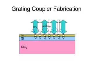
Grating Coupler Fabrication
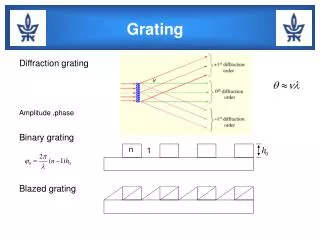
This study explores the fabrication and characterization of grating couplers designed for integrated photonic devices operating at a wavelength of 1.55 µm. The couplers were fabricated using PMMA on silicon substrates, utilizing CF4 and SF6 etching processes, as well as aqua regia for surface preparation. Characterization included SEM and AFM techniques, revealing gratings with periodicities around 730 nm, featuring coupling efficiencies of approximately 10 nm and 20 nm. The results demonstrate promising geometries and efficiencies for applications in photonic crystal waveguides.

Grating Coupler Fabrication
E N D
Presentation Transcript
Grating Coupler Fabrication acetone CF4 e- PMMA Si SiO2
Photonic Crystal Fabrication CF4 dilute aqua regia SF6 e- PMMA Mo Si SiO2
Grating Coupler Geometry For λ = 1.55 µm, ne = 2.83, and θ = 45°, Λ= 730 nm.
Integrated Device SEM 730 nm 426 nm 360 nm