Download
1 / 47
1.84k likes | 4.4k Views
Ion Implantation. M.H.Nemati Sabanci University. Ion Implantation. Introduction Safety Hardware Processes Summary. Introduction. Dope semiconductor Two way to dope Diffusion Ion implantation Other application of ion implantation. Dope Semiconductor: Diffusion. Isotropic process

E N D
Ion Implantation M.H.Nemati Sabanci University
Ion Implantation • Introduction • Safety • Hardware • Processes • Summary
Introduction • Dope semiconductor • Two way to dope • Diffusion • Ion implantation • Other application of ion implantation
Dope Semiconductor: Diffusion • Isotropic process • Can’t independently control dopant profile and dopant concentration • Replaced by ion implantation after its introduction in mid-1970s.
Dope Semiconductor: Ion Implantation • Used for atomic and nuclear research • Early idea introduced in 1950’s • Introduced to semiconductor manufacturing in mid-1970s.
Dope Semiconductor: Ion Implantation • Independently control dopant profile (ion energy) and dopant concentration (ion current times implantation time) • Anisotropic dopant profile • Easy to achieve high concentration dope of heavy dopant atom such as phosphorus and arsenic.
Ion Implantation, Phosphorus P+ SiO2 Poly Si n+ n+ P-type Silicon
Ion Implantation Control • Beam current and implantation time control dopant concentration • Ion energycontrols junction depth • Dopant profile is anisotropic
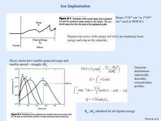
Stopping Mechanism • Ions penetrate into substrate • Collide with lattice atoms • Gradually lose their energy and stop • Two stop mechanisms
Two Stopping Mechanism • Nuclear stopping • Collision with nuclei of the lattice atoms • Scattered significantly • Causes crystal structure damage. • electronic stopping • Collision with electrons of the lattice atoms • Incident ion path is almost unchanged • Energy transfer is very small • Crystal structure damage is negligible
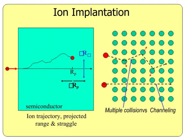
Implantation Processes: Channeling • If the incident angle is right, ion can travel long distance without collision with lattice atoms • It causes uncontrollable dopant profile Lots of collisions Very few collisions
Channeling Effect Lattice Atoms Channeling Ion Collisional Ion q Wafer Surface
Implantation Processes: Channeling • Ways to avoid channeling effect • Tilt wafer, 7° is most commonly used • Screen oxide • Pre-amorphous implantation, Germanium • Shadowing effect • Ion blocked by structures • Rotate wafer and post-implantation diffusion
Implantation Processes: Damage • Ion collides with lattice atoms and knock them out of lattice grid • Implant area on substrate becomes amorphous structure Before Implantation After Implantation
Implantation Processes: Anneal • Dopant atom must in single crystal structure and bond with four silicon atoms to be activated as donor (N-type) or acceptor (P-type) • Thermal energy from high temperature helps amorphous atoms to recover single crystal structure.
Thermal Annealing Lattice Atoms Dopant Atom
Thermal Annealing Lattice Atoms Dopant Atom
Thermal Annealing Lattice Atoms Dopant Atom
Thermal Annealing Lattice Atoms Dopant Atom
Thermal Annealing Lattice Atoms Dopant Atom
Thermal Annealing Lattice Atoms Dopant Atom
Thermal Annealing Lattice Atoms Dopant Atom
Thermal Annealing Lattice Atoms Dopant Atoms
Implantation Processes: Annealing After Annealing Before Annealing
Ion Implantation: Hardware • Gas system • Electrical system • Vacuum system • Ion beamline
Implantation Process Gases and Vapors: P, B, BF3, PH3, and AsH3 Next Step Implanter Select Ion: B, P, As Select Ion Energy Select Beam Current
Ion Implanter Electrical System Gas Cabin Analyzer Magnet Vacuum Pump Ion Source Beam Line Electrical System Vacuum Pump Plasma Flooding System Wafers End Analyzer
Ion Implantation: Gas System • Special gas deliver system to handle hazardous gases • Special training needed to change gases bottles • Argon is used for purge and beam calibration
Ion Implantation: Electrical System • High voltage system • Determine ion energy that controls junction depth • High voltage system • Determine ion energy that controls junction depth • RF system • Some ion sources use RF to generate ions
Ion Implantation: Vacuum System • Need high vacuum to accelerate ions and reduce collision • MFP >> beamline length • 10-5 to 10-7 Torr • Turbo pump and Cryo pump • Exhaust system
Ion Implantation: Control System • Ion energy, beam current, and ion species. • Mechanical parts for loading and unloading • Wafer movement to get uniform beam scan • CPU board control boards • Control boards collect data from the systems, send it to CPU board to process, • CPU sends instructions back to the systems through the control board.
Ion Implantation: Beamline • Ion source • Extraction electrode • Analyzer magnet • Post acceleration • Plasma flooding system • End analyzer
Ion Beam Line Suppression Electrode Analyzer Magnet Vacuum Pump Ion Source Beam Line Extraction Electrode Post Acceleration Electrode Vacuum Pump Plasma Flooding System Wafers End Analyzer
Ion implanter: Ion Source • Hot tungsten filament emits thermal electron • Electrons collide with source gas molecules to dissociate and ionize • Ions are extracted out of source chamber and accelerated to the beamline • RF and microwave power can also be used to ionize source gas
Ion Implantation: Extraction • Extraction electrode accelerates ions up to 50 keV • High energy is required for analyzer magnet to select right ion species.
Ion Implantation: Analyzer Magnet • Gyro radius of charge particle in magnetic field relate with B-field and mass/charge ratio • Used for isotope separation to get enriched U235 • Only ions with right mass/charge ratio can go through the slit • Purified the implanting ion beam
Magnetic Field (Point Outward) Ion Beam Larger m/q Ratio Flight Tube Smaller m/q Ratio Right m/q Ratio Analyzer
Ion Implantation: The Process • CMOS applications • CMOS ion implantation requirements • Implantation process evaluations
Implantation Process: Well Implantation • High energy (to MeV), low current (1013/cm2) P+ Photoresist N-Well P-Epi P-Wafer
Implantation Process: VT Adjust Implantation Low Energy , Low Current B+ Photoresist USG STI P-Well N-Well P-Epi P-Wafer
Lightly Doped Drain (LDD) Implantation • Low energy (10 keV), low current (1013/cm2) P+ Photoresist USG STI P-Well N-Well P-Epi P-Wafer
Implantation Process: S/D Implantation • Low energy (20 keV), high current (>1015/cm2) P+ Photoresist n+ n+ STI USG P-Well N-Well P-Epi P-Wafer
Process Issues • Wafer charging • Particle contamination • Elemental contamination • Process evaluation
Ion Implantation: Safety • One of most hazardous process tools in semiconductor industry • Chemical • Electro-magnetic • Mechanical
Summary of Ion Implantation • Dope semiconductor • Better doping method than diffusion • Easy to control junction depth (by ion energy) and dopant concentration ( by ion current and implantation time). • Anisotropic dopant profile.
Summary of Ion Implantation • Ion source • Extraction • Analyzer magnets • Post acceleration • Charge neutralization system • Beam stop
Summary of Ion Implantation • Well High energy, low current • Source/Drain Low energy, high current • Vt Adjust Low energy, low current • LDD Low energy, low current