Understanding ADCs: Key Definitions and Error Factors
This document provides essential definitions related to Analog-to-Digital Converters (ADCs), including conversion time, number of channels, voltage range, resolution, sampling rate, and various types of errors such as quantization, offset, gain, and nonlinearity errors. It explains fundamental concepts such as sampling theory, the Nyquist criterion, and the impact of sampling speed on signal reconstruction. Furthermore, it discusses how errors can affect ADC performance and methods to mitigate them. This information is vital for professionals working with data acquisition systems.

Understanding ADCs: Key Definitions and Error Factors
E N D
Presentation Transcript
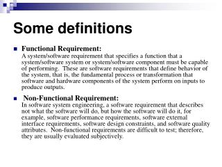
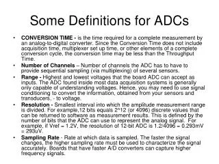
Some Definitions for ADCs • CONVERSION TIME - is the time required for a complete measurement by an analog-to-digital converter. Since the Conversion Time does not include acquisition time, multiplexer set up time, or other elements of a complete conversion cycle, the conversion time may be less than the Throughput Time. • Number of Channels – Number of channels the ADC has to have to provide sequential sampling (via multiplexing) of several sensors. • Range - Highest and lowest voltages that the board ADC can accept as inputs. The ADC found inside most data acquisition systems is generally only capable of understanding voltages. Hence, you may need to use signal conditioning to convert the information, obtained from your sensors and transducers, - to voltage. • Resolution - Smallest interval into which the amplitude measurement range is divided. For example,12 bits equals 2^12 (or 4096) discrete values that can be returned to software as measurement results. This is defined by the number of bits that the ADC can use to represent the analog signal. For example, if Vref = 1.2V, the resolution of 12-bit ADC is 1.2/4096 = 0.293mV = 293uV. • Sampling Rate - Rate at which data is sampled. The faster the signal changes, the higher sampling rate must be used to characterize the signal accurately. Boards that have faster A/D converters can capture higher frequency signals.
SAMPLING THEORY • Samples are snapshots of the changing values (give me your examples) • Sampling has to be done with frequency at least two times more than the highest frequency component in the original (periodic) signal – Nyquist criteria (Harry Nyquist of Bell Telephone Laboratories, 1924) • If sampling is too slow, - reconstruction of the original signal will be wrong. It is called “aliasing”
Errors of ADC • Quantization Error • Offset Error • Gain Error • Differential Linearity Error • Integral Linearity Error • Aperture Error • Total Unadjusted Error (TUE)
Quantization Error • Quantization error is caused by the finite resolution of the ADC, and is an unavoidable imperfection in all types of ADC. The magnitude of the quantization error at the sampling instant is between zero and half of one LSB. • The transfer function of an ideal N-bit ADC is shown in Figure 2.37 (*). The quantization error for any ac signal which spans more than a few LSBs can be approximated by an uncorrelated sawtooth waveform having a peak-to-peak amplitude of q, the weight of an LSB. * See the book’s section 2.3.
Differential and Integral Nonlinearity Errors of ADC • Differential Nonlinearity (DNL): An ideal A/D converter exhibits code transitions at analog input values spaced exactly 1LSB apart (1LSB = VFS / 2^n). DNL is the deviation in code width from the ideal 1LSB code width. A DNL error less than –1LSB can cause missing codes. • DNL is a critical specification for image-processing, closed-loop, and video applications. This is a dc specification, where measurements are taken with near-dc analog input voltages. • Integral Nonlinearity Error is the integral of DLE over the full range.
Offset Error • Offset Error: Offset error is the difference in voltage between the ideal first code transition and the actual code transition of an A/D converter. This is a dc specification, where measurements are taken with near-dc analog input voltages. • In a unipolar device, offset error is the difference between the first measured transition point (lowest in voltage) and the first ideal, transition point. (See Figure 19.) Unipolar Offset Error is measured and calculated as shown in the following equation: Offset Error = (V[0:1]-(0.5)VILSB), where: VILSB – Ideal LSB Voltage, V[0:1] – Analog Voltage of first transition
Unipolar Offset Error Offset Error – difference between actual first code transition point and ideal first code transition point. Offset Error can be calibrated in hardware or FW/SW.
Gain Error • From mathematical expression of the ADC transfer function: D = C + G*A, where: D – digital code, C – offset, G – gain, and A – analog value. • May be defined as the gain error contribution (in mV or LSB) to the total error at full-scale. • Gain can be calibrated out at near full-scale by different measures: changing the transfer function of the sensor or conditioning circuitry, or by changing the voltage reference of the ADC.
Aperture Error (from Wikipedia) • Imagine that we are digitizing a sine wave x(t) = Asin(2πf0t). Provided that the actual sampling time uncertainty due to the clock jitter is Δt, the error caused by this phenomenon can be estimated as Eap <= |X‘(t)∆t| <= 2Aπf0∆t. • The error is zero for DC, small at low frequencies, but significant when high frequencies have high amplitudes. This effect can be ignored if it is drowned out by the quantizing error. Jitter requirements can be calculated using the following formula: , where q is a number of ADC bits.
How the SAR ADC Works • The SAR starts by forcing the MSB (Most Significant bit) high (for example in an 8 bit ADC it becomes 1000 0000 – Why?), the DAC converts it to VAREF/2. The analog comparator compares the input voltage with VAREF/2. If the input voltage is greater than the voltage corresponding to the MSB, the bit is left set, otherwise it is reset. • After this comparison is done, the next significant bit is set (=VAREF/4) and a comparison is done again with the input voltage. The procedure is followed till all the bit positions are compared. • At the end of all the bit comparisons we get the corresponding digital output for the analog input. • The clock frequency must be equal to the sampling frequency multiplied by the number of bits of resolution desired.
How Single Slope ADC Works • Upper Amplifier without feedback works as a comparator. • Bottom Amplifier has a capacitor in the feedback and works as an integrator • MOSFET is needed to reset the integrator • Counter is reset on falling edge (not the level) of the (counter’s) CLR signal • Output buffer is latched on the front edge of the (buffer’s) CLK signal • Counter counts clock signals until CLR goes high
ExpressPCB Installation • Nothing tricky (click OK several times): • www.expresspcb.com
ExpressPCB Installation, Cont. • Happy End:
Concept of SCH Design • Designing the schematic using schematic symbols (from standard library or from yours) • Selecting symbols and placing them on your schematic sheet • Arranging symbols in logical order and connecting them with “wires” • Editing schematic and annotating components • Check schematic for netlist errors command from the File menu
Concept of PCB Design • Designing PCB layout using footprints of components from standard library (or yours) • Selecting footprints from the library and placing them on layout drawing • Arranging footprints in logical order and aligning them using grid (adjustable) • Linking schematic to PCB from the ExpressPCB program's File menu