Download
1 / 36
360 likes | 392 Views
This study presents an evaluation of CMOS and TG logic circuits for implementing a 4-bit ripple carry adder. Performance metrics such as area, propagation delay, power consumption, and glitch behavior are compared through HSPICE simulations. An optimal circuit proposal is detailed following layout and extraction activities. Design requirements, including testing, noise margins, rise and fall times, and layout considerations, are outlined. Guidelines for optimizing TG logic circuitry are presented, emphasizing transistor sizing for efficient operation. Simulation steps and layout validation procedures are addressed to ensure proper functionality and performance metrics.

E N D
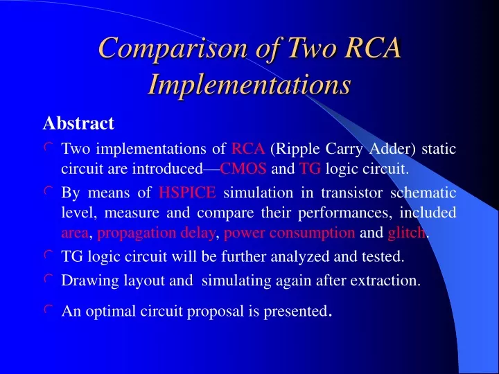
Comparison of Two RCA Implementations Abstract • Two implementations of RCA (Ripple Carry Adder) static circuit are introduced—CMOS and TG logic circuit. • By means of HSPICE simulation in transistor schematic level, measure and compare their performances, included area, propagation delay, power consumption and glitch. • TG logic circuit will be further analyzed and tested. • Drawing layout and simulating again after extraction. • An optimal circuit proposal is presented.
1.1 Background • Transistor-level ASIC cells are the essential element on a single silicon chip, either a small chip or a large chip. • Implement a 4-bit full adder in transistor-level by using CMOS static circuit. • The arithmetic of addition is the most important core parts of processors. • The design of a high performance addition circuit is of prime interest • AT2 is a goal in the project. It means area and delay will be optimized at the same time, but delay takes more weigh.
1.2 Design requirements The aim of the design is a 4-bit full adder. Input two 4-bit numbers A & B. Output is 4-bit sum and a carry. The requirements are given below: 1.Performance Measure: Area-A, Time-T, Power-P, or AT2 as circuit performance 2.Testing: Choose an optimum test vector to test your design
1.2 Design requirements 3.Noise Margins: You are free to choose your logic swing. The noise margins should be at least is 10% of the voltage swing. Make sure you validate this for any gate design you undertake. 4.Rise and Fall times: All input signals and clocks have rise and fall times of less than 500 psec. The rise and fall times of the output signals (10% to 90%) should not exceed 1.5 nsec.
1.2 Design requirements 5.Simulation: Make sure you perform logic simulation, Circuit Simulation, and re_simulate your extracted circuit after circuit extraction 6.Layout: Layout your design fully. Perform DRC (design rules check). Extract your design and simulate it again to obtain your performance measures.
1.2 Design requirements Figure 1.1 Schematic diagram of a 4-bit adder
1.3 Design process Figure 1.2 Design flow
2. A brief introduction to Ripple Carry Adder • 1-bit Full-adder Figure 2.1 Gate schematic for full adder implementation
2. A brief introduction to Ripple Carry Adder • Reuse carry term to implement full adder Figure 2.21bit full adder CMOS complementary implementation
2. A brief introduction to Ripple Carry Adder • Ripple Carry Adder An n-bit adder may be constructed by cascading n 1-bit full-adders, as shown in figure. This is called a Ripple Carry Adder. It is one kind of bit-parallel adder.
3. Comparison of CMOS and TG Logic • Implementation and optimization CMOS complementary implementation: single-bit full-adder is implemented according to above two figures. The carry will be reused to reduce the circuit area, so the carry block cascade with the sum block to compose one single-bit full-adder cell.
3.Comparison of CMOS and TG Logic • Implementation and optimization Transmission Gate implementation: the implementation of single-bit transmission gate full-adder is rather different from CMOS. Its basic element is an exclusive-or (XOR) gate. The schematic for this XOR is shown in below figure. By reversing the connections of A and –A, an exclusive-nor (XNOR) gate is constructed.
3.Comparison of CMOS and TG Logic • Implementation and optimization (a) XOR Gate (b) Logic architecture Figure 3.1 Transmission Gate implementation
3. Comparison of CMOS and TG Logic • Optimizations guideline 1. Arrange the transistors switched by the carry in signal (C) close to the output. This will enable the input signals to settle the gate such that the C transistors are least influenced by body effect. 2. Make all transistors in the sum gate whose gate signals are connected to CARRY minimum size. This minimizes the capacitive load on this signal. Keep routing on this signal to a minimum and minimize the use of diffusion as a routing layer.
3.Comparison of CMOS and TG Logic • Optimizations guideline 3.Sizing of series transistors can be determined by simulation. It may or may not pay to increase size of the series n-transistors and p-transistors. For instance, it may not pay to increase the size of the series transistors connected to A and B in the carry gate in a ripple carry adder, because these signals will have time to settle in the upper bits of the adder while the carry is rippling. It may be of advantage to increase the size of the C transistors in the carry gate to override the effects of stray capacitance. For a parallel adder, the SUM gate transistors may be make minimum size.
3.Comparison of CMOS and TG Logic • Optimizations guideline 4. It is difficult to size the transmission gate logic. The best way is to do simulation. 5.Increasing the buffer size can refine the output waves shape and eliminate glitch efficiently. However, the drawback is increment of the propagation delay.
3.Comparison of CMOS and TG Logic • Simulation result • The simulation is done in HSPICE Level3 Model, 0.5μm process. -Simulation environment setting: • Temperature: 25℃ • Power supply voltage: 3.3 Volt
3.Comparison of CMOS and TG Logic • Simulation result -Test vector Time: from=0ns, to=100ns Pulse width: 5ns Input tr&tf (rise time and fall time): case1—10ps, case2—250ps
3.Comparison of CMOS and TG Logic • Simulation result The test vector is determined by the following factor: 1. Check the circuit input and output logic functions properly. 2. Measure the average and transient power value relative accurate. 3. Include the worst-case input to determine the delay.
3.Comparison of CMOS and TG Logic • Simulation result Table 3.1 4-bit RCA performance comparison of CMOS and TG logic (min size)
3.Comparison of CMOS and TG Logic • Simulation result Table 3.2 4-bit RCA performance comparison of CMOS and TG logic (Wp/Wn=2/1)
3.Comparison of CMOS and TG Logic • Simulation result Note: 1. Assume all transistor’s drain and source length Ls=Ld=1μm, width W=Wmin. 2. Transistor’s area=Area|gate+Area|drain+Area|source 3. The buffer size has been readjusted in terms of the glitch of the output wave. 4. Propagation delay (Tp) is counted from the first input time to the last output time. In the case of CMOS logic, the first input is A(0) or Cin, the last output is SUM(3). Measure from 50%voltage to 50%voltage. 5. Delay is examined in the worst case.
4. Analysis of simulation result • Delay Figure 4.1 Critical path in a 4-bit ripple-carry adder Note: delay from carry-in to carry-out is more important than from A to carry-out or from carry-in to SUM, because the carry-propagation chain will determine the latency of the whole circuit for a Ripple-Carry adder.
4. Analysis of simulation result • Delay The latency of a 4-bit ripple carry adder can be derived by considering the above worst-case signal propagation path. We can thus write the following expression: TRCA-4bit = TFA(A0,B0→Cout)+2* TFA (Cin→Cout)+TFA (Cin→S3) And, it is easy to extend to k-bit RCA: TRCA-4bit = TFA(A0,B0→Cout)+(K-2)* TFA (Cin→Cout)+TFA (Cin→Sk-1)
4. Analysis of simulation result • Delay Table 4.1 Simulation delay of 1-bit full adder (min size)
4.Analysis of simulation result • Delay -Comparing the simulation result in Table3.1 the case of 4-bit RCA, the propagation delay of CMOS logic is faster than that of TG logic. -Carry delay of CMOS logic is smaller than that of TG logic -TG logic is more sensitive for the input slope than the CMOS logic from the point of view delay.
4. Analysis of simulation result • Power Dissipation -The average power consumption is given by Where Tis the computing period, which is set to 100ns in program; Pt is the circuit transition power -The simulation result indicates the power dissipation of CMOS logic is lightly smaller than that of TG logic. • Area -The number of transistor of TG logic is less than that of CMOS logic, so its area is smaller.
4. Analysis of simulation result • AT, AT2,DP These products are commonly used to evaluate one circuit performance. A=Area, T=Time (delay),D=Delay, P=Power Choosing one or some of these products for one circuit’s performance specifications: -The CMOS logic has better performance in AT and AT2 measurement -CMOS and TG logic almost have the same weigh in DPmeasurement -CMOS logic shows more advantages in performance AT and AT2due to smaller delay of carry-in to carry-out in a long series 1-bit adder chain. -the performance of sized TG logic (Wp/Wn=2/1) approaches the minimum size CMOS in AT and AT2.
4. Analysis of simulation result • Decision So far, we discuss several simulation results of CMOS and TG logic static circuit for a 4-bit ripple-carry adder. They both have advantages and disadvantages in the different ways. From the point of view of AT2, CMOS logic outweighs TG logic. It is known that CMOSlogic has the minimum propagation delay when its Wp/Wn=(μn/μp)1/2 TG logic (optimized delay) for our ultimate scheme to do the further simulation to validate this hypothesis
5. Layout Analysis • Layout consideration The main objective associated with layout design is to obtain a circuit with optimum yield as small an area as possible without compromising reliability of circuit. Design rules represent the best possible compromise between performance and yield. The more conservative the rules are, the more likely it is that the circuit will function. The flow of design is 1-bit adder layout → 4-bit adder layout → I/O drivers and PADs.
5. Layout Analysis • Layout consideration 1 bit adder layout (Area: 45x28μm2 )
5. Layout Analysis • Layout consideration 4 bits adder layout (Area: 102x62μm2 )
5. Layout Analysis • Post-Layout simulation result Extract from layout to generate the corresponding cell and carry out its simulation
5. Layout Analysis • Post-Layout simulation result Extract from layout to generate the corresponding cell and carry out its simulation Table5.1 Post-layout Simulation results and circuit specifications(4bit adder) The result shows the big difference in power consumption between schematic simulation and post-layout simulation.
6. Conclusion • Two logic structures, CMOS complementary and Transmission Gate for design a 4-bit ripple-carry adder • Two schemes (normal and optimized) are used to construct the different circuit for each logic structure respectively. • Compare their performance such as delay and power dissipation by simulation. They exhibit advantages and disadvantages in different aspects • For the case of 4-bit ripple-carry adder, TG logic shows the smaller area, and CMOS logic illustrates the better performance in delay, AT, AT2, and little difference in power consumptions. • For either CMOS logic or TG logic, it is necessary to size the transistor to get the optimum performance parameter • TG logic can construct a circuit more flexibly, for instance it is easy to have the inverted or non-inverted signal in the output, whereas CMOS logic only has the inverted signal output. • When the slope of input signal is changed, TG logic is sensitive in delay, whereas CMOS logic is sensitive in glitch.