Download
1 / 46
460 likes | 527 Views
Explore static elaboration in Verilog with parameterization, generating modules, and combining parameters for powerful elaboration techniques. Learn through practical examples and behavioral modeling.

E N D
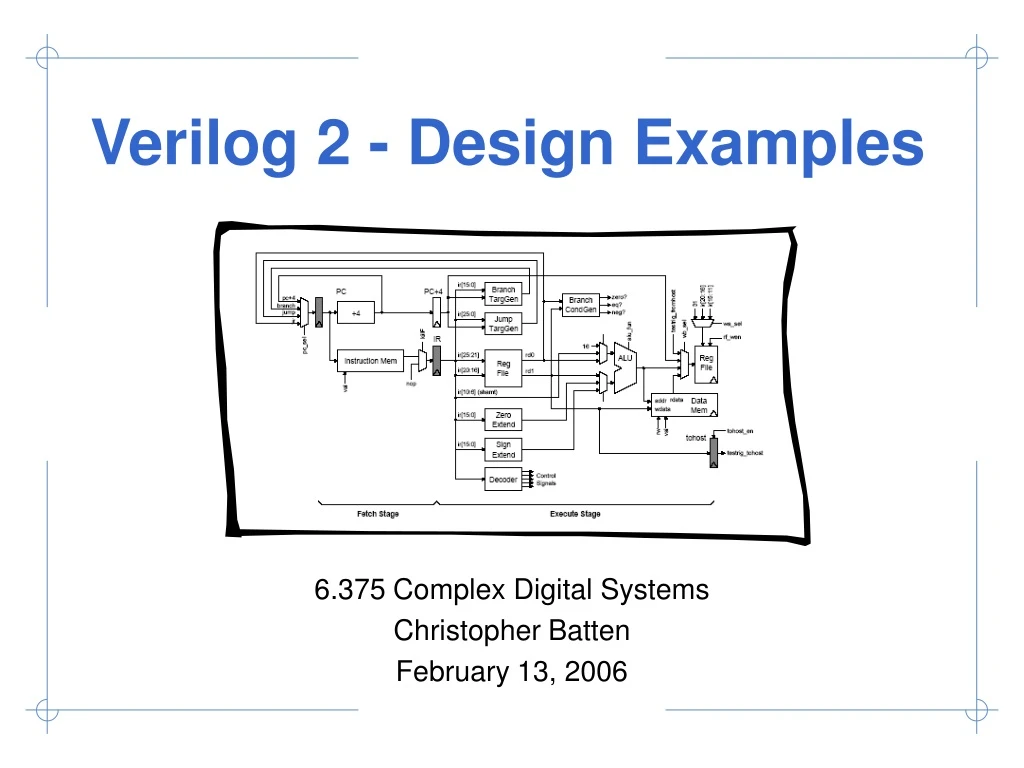
Verilog 2 - Design Examples 6.375 Complex Digital Systems Christopher Batten February 13, 2006
Course administrative notes • If you did not receive an email over the weekend concerning the course then you are not on the student mailing list - please email 6.375-staff • Lab 1 has been posted on the course website. It is due Friday, February 24 • 2-stage SMIPSv2 processor RTL checked into CVS • Critical thinking questions • Tutorials on VCS, CVS, and SMIPS assembly programming will be posted this week
Verilog Design Examples • Parameterized Static Elaboration • Greatest Common Divisor • Unpipelined SMIPSv1 processor
Static elaboration enables generation of hardware at synthesis time We will look at two forms of static elaboration: (1) parameters and (2) generate blocks Register Transfer Level Static Elaboration Simulate Test Results Elaborated Design Logic Synthesis Simulate Test Results Gate Level Auto Place + Route
Parameters are bound during static elaboration creating flexible modules module vcMux2 #( parameterWIDTH = 1 ) ( input [WIDTH-1:0] in0, in1, input[1:0] sel, output[WIDTH-1:0] out ); always @(*) begin case ( sel ) 1’d0 : out = in0; 1’d1 : out = in1; default : out = {WIDTH{1’bx}}; endcase end endmodule Instantiation Syntax vcMux2#(32) alu_mux ( .in0 (op1), .in1 (bypass), .sel (alu_mux_sel), .out (alu_mux_out) );
Parameters are bound during static elaboration creating flexible modules module vcERDFF_pf #( parameterWIDTH = 1, parameterRESET_VALUE = 0 ) ( input clk, input reset, input [WIDTH-1:0] d, input en, outputreg[WIDTH-1:0] q ); always @( posedge clk ) if ( reset ) q <= RESET_VALUE; elseif ( en ) q <= d; endmodule Instantiation Syntax vcERDFF_pf#(32,32’h10) pc_pf ( .clk (clk), .reset (reset), .en (pc_enable), .d (pc_mux_out), .q (pc) );
All genvars must be disappear after static elaboration Generated names will have ripple[i]. prefix Generate blocks can execute loops and conditionals during static elaboration module adder ( input [3:0] op1,op2, output cout, output[3:0] sum ); wire [4:0] carry; assign carry[0] = 1’b0; assign cout = carry[4] genvar i; generate for ( i = 0; i < 4; i = i+1 ) begin : ripple FA fa( op1[i], op2[i], carry[i], carry[i+1] ); end endgenerate endmodule
Combining parameters + generate blocks enables more powerful elaboration module adder#( parameterWIDTH = 1 ) ( input [WIDTH-1:0] op1,op2, output cout, output[WIDTH-1:0] sum ); wire [WIDTH:0] carry; assign carry[0] = 1’b0; assign cout = carry[WIDTH]; genvar i; generate for ( i = 0; i < WIDTH; i = i+1 ) begin : ripple FA fa( op1[i], op2[i], carry[i], carry[i+1] ); end endgenerate endmodule Use parameter for loop bounds
Generate statements are useful for more than just module instantiation module adder#( parameterWIDTH = 1 ) ( input [WIDTH-1:0] op1,op2, output cout, output[WIDTH-1:0] sum ); wire [WIDTH:0] carry; assign carry[0] = 1’b0; assign cout = carry[WIDTH]; genvar i; generate for ( i = 0; i < WIDTH; i = i+1 ) begin : ripple assign {carry[i+1],sum[i]} = op1[i] + op2[i] + carry[i]; end endgenerate endmodule Statically elaborating many continuous assignments
Traditionally designers have resorted to behavioral inference for elaboration module adder#( parameterWIDTH = 1 ) ( input [WIDTH-1:0] op1,op2, output cout, outputreg[WIDTH-1:0] sum ); wire [WIDTH:0] carry; assign cout = carry[WIDTH]; integer i; always @(*) begin assign carry[0] = 1’b0; for ( i = 0; i < WIDTH; i = i+1 ) {carry[i+1],sum[i]} = op1[i] + op2[i] + carry[i]; end end endmodule Although similar to generate block, this code has very different semantics!
Verilog Design Examples • Parameterized Static Elaboration • Greatest Common Divisor • Unpipelined SMIPSv1 processor
Behavioral GCD model is written within a single always block with C like structure module gcdGCDUnit_behav#( parameter W = 16 ) ( input[W-1:0] inA, inB, output[W-1:0] out ); reg [W-1:0] A, B, out, swap; integer done; always@(*) begin done = 0; A = inA; B = inB; while ( !done ) begin if ( A < B ) swap = A; A = B; B = swap; elseif ( B != 0 ) A = A - B; else done = 1; end out = A; end endmodule Test harness will simply set the input operands and check the output.
Simple test harness for behavioral model of GCD module exGCDTestHarness_behav; reg [15:0] inA, inB; wire [15:0] out; exGCD_behav#(16) gcd_unit( .inA(inA), .inB(inB), .out(out) ); initial begin // 3 = GCD( 27, 15 ) inA = 27; inB = 15; #10; if ( out == 3 ) $display( "Test ( gcd(27,15) ) succeeded, [ %x == %x ]", out, 3 ); else $display( "Test ( gcd(27,15) ) failed, [ %x != %x ]", out, 3 ); $finish; end endmodule
State Less-Than Comparator Equal Comparator Subtractor Behavioral GCD model is written within a single always block with C like structure module gcdGCDUnit_behav#( parameter W = 16 ) ( input[W-1:0] inA, inB, output[W-1:0] Y ); reg [W-1:0] A, B, Y, swap; integer done; always@(*) begin done = 0; A = inA; B = inB; while ( !done ) begin if ( A < B ) swap = A; A = B; B = swap; elseif ( B != 0 ) A = A - B; else done = 1; end Y = A; end endmodule Our goal now is to design an RTL hardware block which implements this high-level behavior. What does the RTL implementation need?
operands_val result_val operands_rdy result_rdy operands_bits_A result_bits_data operands_bits_B clk reset The first step is to carefully design an appropriate port interface
zero? lt A Next develop a datapath which has the proper functional units A = inA; B = inB; while ( !done ) begin if ( A < B ) swap = A; A = B; B = swap; elseif ( B != 0 ) A = A - B; else done = 1; end Y = A; B
zero? lt A Next develop a datapath which has the proper functional units A = inA; B = inB; while ( !done ) begin if ( A < B ) swap = A; A = B; B = swap; elseif ( B != 0 ) A = A - B; else done = 1; end Y = A; B
zero? lt A sub Next develop a datapath which has the proper functional units A = inA; B = inB; while ( !done ) begin if ( A < B ) swap = A; A = B; B = swap; elseif ( B != 0 ) A = A - B; else done = 1; end Y = A; B
A mux sel A reg en B mux sel B reg en B = 0 A < B zero? lt A sub Finally add the control unit to sequence the datapath A = inA; B = inB; while ( !done ) begin if ( A < B ) swap = A; A = B; B = swap; elseif ( B != 0 ) A = A - B; else done = 1; end Y = A; B
A sel A en B sel B en B = 0 A < B zero? lt A sub B Datapath module interface module gcdGCDUnitDpath_sstr#( parameter W = 16 ) ( input clk, // Data signals input [W-1:0] operands_bits_A, input [W-1:0] operands_bits_B, output [W-1:0] result_bits_data, // Control signals (ctrl->dpath) input A_en, input B_en, input [1:0] A_mux_sel, input B_mux_sel, // Control signals (dpath->ctrl) output B_zero, output A_lt_B );
A sel A en B sel B en B = 0 A < B zero? lt A sub B Try to contain all functionality in leaf modules wire [W-1:0] B; wire [W-1:0] sub_out; wire [W-1:0] A_mux_out; vcMux3#(W) A_mux ( .in0 (operands_bits_A), .in1 (B), .in2 (sub_out), .sel (A_mux_sel), .out (A_mux_out) ); wire [W-1:0] A; vcEDFF_pf#(W) A_pf ( .clk (clk), .en_p (A_en), .d_p (A_mux_out), .q_np (A) );
Using explicit state helps eliminate issues with non-blocking assignments Continuous assignment combinational logic is fine Try to contain all functionality in leaf modules wire [W-1:0] B_mux_out; vcMux2#(W) B_mux ( .in0 (operands_bits_B), .in1 (A), .sel (B_mux_sel), .out (B_mux_out) ); vcEDFF_pf#(W) B_pf ( .clk (clk), .en_p (B_en), .d_p (B_mux_out), .q_np (B) ); assign B_zero = ( B == 0 ); assign A_lt_B = ( A < B ); assign sub_out = A - B; assign result_bits_data = A; wire [W-1:0] B; wire [W-1:0] sub_out; wire [W-1:0] A_mux_out; vcMux3#(W) A_mux ( .in0 (operands_bits_A), .in1 (B), .in2 (sub_out), .sel (A_mux_sel), .out (A_mux_out) ); wire [W-1:0] A; vcEDFF_pf#(W) A_pf ( .clk (clk), .en_p (A_en), .d_p (A_mux_out), .q_np (A) );
Control unit requires a simple state machine for valid/ready signals reset WAIT Waiting for new input operands operands_val CALC Swapping and subtracting !( A < B ) & ( B = 0 ) DONE Waiting for consumer to take the result result_rdy
Implementing the control logic finite state machine in Verilog localparam WAIT = 2'd0; localparam CALC = 2'd1; localparam DONE = 2'd2; reg [1:0] state_next; wire [1:0] state; vcRDFF_pf#(2,WAIT) state_pf ( .clk (clk), .reset_p (reset), .d_p (state_next), .q_np (state) ); Localparams are not really parameters at all. They are scoped constants. Explicit state in the control logic is also a good idea!
WAIT : begin A_mux_sel = A_MUX_SEL_IN; A_en = 1'b1; B_mux_sel = B_MUX_SEL_IN; B_en = 1'b1; operands_rdy = 1'b1; end CALC : if ( A_lt_B ) A_mux_sel = A_MUX_SEL_B; A_en = 1'b1; B_mux_sel = B_MUX_SEL_A; B_en = 1'b1; elseif ( !B_zero ) A_mux_sel = A_MUX_SEL_SUB; A_en = 1'b1; end DONE : result_val = 1'b1; Implementing the control signal outputs for the finite state machine reg [6:0] cs; always@(*) begin // Default control signals A_mux_sel = A_MUX_SEL_X; A_en = 1'b0; B_mux_sel = B_MUX_SEL_X; B_en = 1'b0; operands_rdy = 1'b0; result_val = 1'b0; case ( state ) WAIT : ... CALC : ... DONE : ... endcase end
reset WAIT operands_val CALC !( A < B ) & ( B = 0 ) DONE result_rdy Implementing the state transitionsfor the finite state machine always @(*) begin // Default is to stay in the same state state_next = state; case ( state ) WAIT : if ( operands_val ) state_next = CALC; CALC : if ( !A_lt_B && B_zero ) state_next = DONE; DONE : if ( result_rdy ) state_next = WAIT; endcase end
RTL test harness requires properly handling the ready/valid signals Generic Test Source Generic Test Sink A sel A en B sel B en B = 0 A < B zero? lt A sub B
We can compare the behavioral and RTL implementations to verify correctness Test Inputs Behavioral Model RTL Model Test Outputs Test Outputs Identical?
Verilog Design Examples • Parameterized Static Elaboration • Greatest Common Divisor • Unpipelined SMIPSv1 processor
SMIPS is a simple MIPS ISA which includes three variants • SMIPSv1 • 5 instructions • No exceptions/interrupts • Lecture examples • SMIPSv2 • 35 instructions • No exceptions/interrupts • ISA for lab assignments • SMIPSv3 • 58 instructions • Full system coproc with exceptions/Interrupts • Optional ISA for projects
The first step is to carefully design an appropriate port interface
SMIPSv1 Block DiagramHow do we start implementing? Divide and Conquer! Step 1: Identify the memories Step 2: Identify the datapaths Step 3: Everything else is random logic
Word Lines Single memory bit cell Single full adder bit Data Flow Control Flow Bit Lines Why memories, datapath, and control? To exploit the structure inherent in each
2KB Instruction Cache Control Regfile Tags Datapath Stanford MIPS-X5 Stage, 20MHz RISC Processor
Vector Datapaths Dpath Ctrl Ctrl I$ Berkeley T08 Lane Vector Microprocessor
Control Reg File 8 Dpaths Stanford ImagineStreaming Application Engine
Switch ICache Network FIFOs X FP Ctrl ICache DCache MIT RAW16 Tiled General Purpose Processor
Pure cell-based ASIC flows can no longer ignore the importance of partitioning
Let’s identify the memories, datapaths, and random logic in our SMIPSv1 design Divide and Conquer! Step 1: Identify the memories Step 2: Identify the datapaths Step 3: Everything else is random logic
Let’s identify the memories, datapaths, and random logic in our SMIPSv1 design Now identify the signals which will make up the interface between the datapath, memories, and random logic
SMIPSv1 datapath interface contains controls signals and memory data buses module smipsProcDpath_pstr ( input clk, reset, // Memory ports output [31:0] imemreq_bits_addr, output [31:0] dmemreq_bits_addr, output [31:0] dmemreq_bits_data, input [31:0] dmemresp_bits_data, // Controls signals (ctrl->dpath) input pc_mux_sel, input [ 4:0] rf_raddr0, input [ 4:0] rf_raddr1, input rf_wen, input [ 4:0] rf_waddr, input op0_mux_sel, input op1_mux_sel, input [15:0] inst_imm, input wb_mux_sel, // Control signals (dpath->ctrl) output branch_cond_eq, output[7:0] tohost_next ); wire [31:0] branch_targ; wire [31:0] pc_plus4; wire [31:0] pc_mux_out; vcMux2#(32) pc_mux ( .in0 (pc_plus4), .in1 (branch_targ), .sel (pc_mux_sel), .out (pc_mux_out) ); wire [31:0] pc; vcRDFF_pf#(32,32'h0001000) pc_pf ( .clk (clk), .reset_p (reset), .d_p (pc_mux_out), .q_np (pc) ); assign imemreq_bits_addr = pc; vcInc#(32,32'd4) pc_inc4 ( .in (pc), .out (pc_plus4) );
Register file with two combinational read ports and one write port module smipsProcDpathRegfile ( input clk, input [ 4:0] raddr0, // Read 0 address (combinational input) output [31:0] rdata0, // Read 0 data (combinational on raddr) input [ 4:0] raddr1, // Read 1 address (combinational input) output [31:0] rdata1, // Read 1 data (combinational on raddr) input wen_p, // Write enable (sample on rising clk edge) input [ 4:0] waddr_p, // Write address (sample on rising clk edge) input[31:0] wdata_p // Write data (sample on rising clk edge) ); // We use an array of 32 bit register for the regfile itself reg [31:0] registers[31:0]; // Combinational read ports assign rdata0 = ( raddr0 == 0 ) ? 32'b0 : registers[raddr0]; assign rdata1 = ( raddr1 == 0 ) ? 32'b0 : registers[raddr1]; // Write port is active only when wen is asserted always@( posedge clk ) if ( wen_p && (waddr_p != 5'b0) ) registers[waddr_p] <= wdata_p; endmodule
Verilog for SMIPSv1 control logic `define LW 32'b100011_?????_?????_?????_?????_?????? `define SW 32'b101011_?????_?????_?????_?????_?????? `define ADDIU 32'b001001_?????_?????_?????_?????_?????? `define BNE 32'b000101_?????_?????_?????_?????_?????? localparam cs_sz = 8; reg [cs_sz-1:0] cs; always @(*) begin cs = {cs_sz{1'b0}}; casez ( imemresp_bits_data ) // op0 mux op1 mux wb mux rfile mreq mreq tohost // br type sel sel sel wen r/w val en `ADDIU : cs = { br_pc4, op0_sx, op1_rd0, wmx_alu, 1'b1, mreq_x, 1'b0, 1'b0 }; `BNE : cs = { br_neq, op0_sx2, op1_pc4, wmx_x, 1'b0, mreq_x, 1'b0, 1'b0 }; `LW : cs = { br_pc4, op0_sx, op1_rd0, wmx_mem, 1'b1, mreq_r, 1'b1, 1'b0 }; `SW : cs = { br_pc4, op0_sx, op1_rd0, wmx_x, 1'b0, mreq_w, 1'b1, 1'b0 }; `MTC0 : cs = { br_pc4, op0_x, op1_x, wmx_x, 1'b0, mreq_x, 1'b0, 1'b1 }; endcase end casez performs simple pattern matching and can be very useful when implementing decoders
Verilog for SMIPSv1 control logic // Set the control signals based on the decoder output wire br_type = cs[7]; assign pc_mux_sel = ( br_type == br_pc4 ) ? 1'b0 : ( br_type == br_neq ) ? ~branch_cond_eq : 1'bx; assign op0_mux_sel = cs[6]; assign op1_mux_sel = cs[5]; assign wb_mux_sel = cs[4]; assign rf_wen = ( reset ? 1'b0 : cs[3] ); assign dmemreq_bits_rw = cs[2]; assign dmemreq_val = ( reset ? 1'b0 : cs[1] ); wire tohost_en = ( reset ? 1'b0 : cs[0] ); // These control signals we can set directly from the instruction bits assign rf_raddr0 = inst[25:21]; assign rf_raddr1 = inst[20:16]; assign rf_waddr = inst[20:16]; assign inst_imm = inst[15:0]; // We are always making an imemreq assign imemreq_val = 1'b1;
Take away points • Parameterized models provide the foundation for reusable libraries of components • Use explicit state to prevent unwanted state inference and to more directly represent the desired hardware • Begin your RTL design by identifying the external interface and then move on to partition your design into the memories, datapaths, and control logic Next Lecture: We will discuss CMOS technology issues including gates, wires, and circuits