Download
1 / 8
80 likes | 291 Views
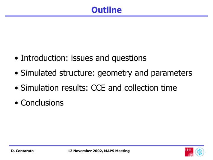
Outline. Introduction: issues and questions Simulated structure: geometry and parameters Simulation results: CCE and collection time Conclusions. D. Contarato. 12 November 2002, MAPS Meeting. Introduction. Issues The feasibility of the sensors in a deep-submicron technology implies:

E N D
Outline • Introduction: issues and questions • Simulated structure: geometry and parameters • Simulation results: CCE and collection time • Conclusions D. Contarato 12 November 2002, MAPS Meeting
Introduction • Issues • The feasibility of the sensors in a deep-submicron technology implies: • reduced epilayer thickness (smaller sensitive volume) • presence of isolation structures (Shallow Trench Isolation) • radiation hardness (build-up of radiation-induced interface states) • Questions • How does the reduction of the epilayer thickness influence the signal? • How does radiation-induced interface states influence the charge collection properties? • How does the geometry of the isolation structures influence the charge collection, in particular with respect to interface damage? D. Contarato 12 November 2002, MAPS Meeting
Simulated structure • 2D model of a 3-pixels “cluster” • Pixel pitch 20 mm; diode width 1 mm • Epilayer thickness was varied between 2 and 8 mm • “General purpose” doping profiles (typical values, from literature) • The structure was simulated both with and without Shallow Trench Isolation (STI) • Trench width (TW): 1 – 2 mm. Trench depth (TD): 0.2 – 0.5 mm (values of geometrical parameters are… guessed!) • Interface traps concentrations: 1011, 10121/eVcm2, roughly equivalent to a dose up to ~500 krad (Wüstenfeld 2001, Ph.D. thesis) • Shallow donor- and acceptor-like traps taken into consideration D. Contarato 12 November 2002, MAPS Meeting
Charge collection without STI • Linear dependence of collected signal on epilayer thickness • The substrate contribution is almost constant?! • Signal is poor for thinner epilayer: the charge spreading between adjacent pixels is anyway limited • A thinner epilayer results in shorter collection times, but even at the thickest values the collection time is well below 100 ns (first MIMOSA prototypes, 15 mm epilayer) D. Contarato 12 November 2002, MAPS Meeting
CCE vs Interface Traps (no STI) • The decrease of the CCE after ~500 krad is of about 6-7% • The collection times are not significantly affected • No intuitive explanation of the effect! D. Contarato 12 November 2002, MAPS Meeting
CCE: comparison NoSti vs. Sti (“PreRad”) Slight decrease of CCE (~4%) with the presence of STI even without the introduction of traps, showing a dependence on trench depth (but not on trench width) The general trend is an increase of the collection time in the presence of STI (how does the oxide influence the electric field?) D. Contarato 12 November 2002, MAPS Meeting
CCE vs Interface Traps, with STI Epi 2 um Epi 5 um • Significant dependence of collected charge on trench depth (with a bigger trench depth also the effect of the lowest trap concentration becomes sensible) • Collection times are not affected Epi 8 um D. Contarato 12 November 2002, MAPS Meeting
Conclusions • Thinner epilayer: poor signal, but limited charge spreading, shorter collection times (faster collection), and reduced effect of interface damage • Thicker epilayer: better signal, collection times still ok, but bigger charge losses after introduction of interface states • In the presence of interface damage, there is a sensible dependence of the collected charge on the trench geometry (mainly on depth) D. Contarato 12 November 2002, MAPS Meeting