Download
1 / 18
210 likes | 573 Views
Resistance Temperature detector (RTD) project. Dr. Hisham E. Hegab College of Engineering & Science Louisiana Tech University Ruston, LA hhegab@latech.edu. RTD Sensor Overview. Students: Design geometry Create mask pattern using CAD package Perform photolithography

E N D
Resistance Temperature detector (RTD) project Dr. Hisham E. Hegab College of Engineering & Science Louisiana Tech University Ruston, LA hhegab@latech.edu Living with the Lab Workshop – July 14th, 2009
RTD Sensor Overview Students: • Design geometry • Create mask pattern using CAD package • Perform photolithography • Inspect resulting device • Test and calibrate their senor Living with the Lab Workshop – July 14th, 2009
Project Logistics/Organization Organization • Class size up to 40 students • Each student designs an RTD pattern & creates their own corresponding mask pattern • Optical lithography performed in teams of 4 students but yields up to 6 RTDs per team • Calibration performed in teams of 2 students • Focused on having as much “hands-on” as possible Living with the Lab Workshop – July 14th, 2009
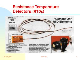
Project Overview/RTD Design • Introduction to temperature & its measurement • Look at different types of sensors • Advantages/disadvantages • Focus on RTDs • Types (film vs. wire coil) • Materials used • Relevant fundamentals • Brief overview of design • Nickel film resistor design • Use glass substrate • 200 nm Ni film on 2-3 nm Cr • pattern using optical photolithography • Use RCTime circuit to sense resistance change of sensor Living with the Lab Workshop – July 14th, 2009
1st Homework Assignment • Students asked to design the geometry required to produce a 100 W RTD using a 200 nm thick nickel film. • Also required to create a spreadsheet predicting its resistance vs. temperature (determine its sensitivity) • Also assigned to create a mask pattern for fabricating their design • Masks are fabricated using a high resolution printer (imagesetter) – performed by teaching assistant Living with the Lab Workshop – July 14th, 2009
Microfabrication Lecture – 2nd class period • Provides background information on processing steps involved in photolithography • Students learn about chemicals involved (e.g., photoresists, developer, etchants) and safety considerations • Students perform all steps in fabrication except Ni etching (nitric acid) and dicing RTDs (glass cutting) Fabrication Steps • Prepare the substrate for spinning • Spin the photoresist • Soft bake • Apply a photomask and expose to UV light • Develop the photoresist • Rinse and dry • Hard bake • Etch • Remove photoresist • Dice individual RTDs • Inspect resistor pattern • Connect leads • Seal sensor Living with the Lab Workshop – July 14th, 2009
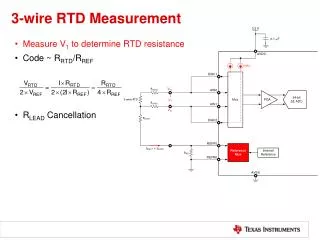
Review RC Time Circuit • Students use RC time circuit to measure resistance of detector • Have already been exposed to the basics of this measurement circuit in previous ENGR 120 course • Provide brief review • Now asked to look at what values of R1 and C would make their sensor perform the best Living with the Lab Workshop – July 14th, 2009
Fabrication – Class Period 3 & 4 • Provide students with step by step set of PowerPoint slides • Slides contain explicit instructions for equipment as well as relevant safety warnings • Lab room adjacent to classroom equipped with spinner, UV exposure station, hot plates & developing station Living with the Lab Workshop – July 14th, 2009
Before beginning the fabrication process put on latex gloves and a pair of safety glasses. The gloves are used primarily to help keep the substrate you will be handling clean. Handle the substrate using tweezers and/or holding it by its edges so that you do not get dust or dirt on the surface. Dirt can cause imperfections in the transfer of the RTD pattern while doing photolithography. We will be using photoresist, MF-319 developer, and de-ionized (DI) water during the fabrication. While none of these chemicals are extremely hazardous, you should wear safety goggles to protect your eyes at all times. The developer is flammable so do not place it near the hot plate or any other source of heat. Safety Precautions Before You Begin!
Your instructor and/or a lab assistant should provide you with a substrate packaged in a plastic container. The substrate is a 50 mil thick microscope glass slide with a 3-5 nm layer of chromium and a 200 nm layer of nickel deposited on it. We will create 6 RTD patterns on one 2" x 3" slide and then separate the individual RTDs after they have been patterned and etched. The substrate is already clean so it is ready to start the fabrication process. Obtain Substrate Nickel Chromium Glass
Place Substrate in Spinner Lift the lid of the spinner and using tweezers place the substrate onto the chuck of the spinner. Align Substrate Center the substrate on the chuck by placing your fingers on both sides of the substrate.
Mask Alignment After the soft bake, place the substrate inside the UV exposure station. Then place your mask pattern on top of the substrate. Be careful to align the mask pattern to the edges of your substrate.
Exposure Place a glass plate over your mask/substrate. The plate applies pressure to the mask so that it sits firmly on the substrate during the exposure process. Place the back edge of the glass plate down inside the UV station and lower the front edge into place so that you do not disturb the alignment of the mask. Close the chamber door and press the enter button to expose the mask/substrate for 120 seconds.
Develop the Photoresist Remove the substrate from the UV exposure station and take it to the developer tray. There are two small baths in the developer tray. One contains MF-319 developer and the other contains DI water. Holding the substrate with tweezers gently wash the substrate in the developer bath. Make sure to completely submerge it in the developer so that it will develop the substrate evenly. Take it out every 5 seconds to see if the developer has washed the photoresist away (“rainbow” or multi-colored areas that were exposed to UV light should disappear). As soon as it appears to be fully developed, dip the substrate into the DI water bath to stop the development process.
Inspection & Final Fab – Class Period 5 • Perform optical inspection • Check continuity & room temperature resistance • Solder lead wires • Seal RTD right amount of exposed wire Living with the Lab Workshop – July 14th, 2009
Calibration/Testing – Class Period 6 • Outside of class (HW) students design/build RC Time circuit to measure resistance of their RTD – affects sensitivity • Calibration performed using water bath stations provided by temperature controlled hot plates • Perform regression analysis as homework Living with the Lab Workshop – July 14th, 2009
Equipment & Facilities Dedicated Facilities & Equipment: • Automated dispensing spinner (~$6K) • Timer controlled UV oven ($3K) • Hot plates (~$1K/each, need ~3-4/lab) • Shop microscopes (~$150/each, 1 per 4 students) • Mask printer (~$8K or can be outsourced ~$25/class) • Clean air hood (~$3K) • Clean, dry air • Fume hood for etching (~$15-25K) Consumables: • Chemicals, glass slides, lead wires, sealing epoxy (~$3-5/student) Other Implementation Options: • Masks could be printed with high resolution laser printer • Could limit photolithography to demonstrations • Use available temperature sensor from parallax Living with the Lab Workshop – July 14th, 2009