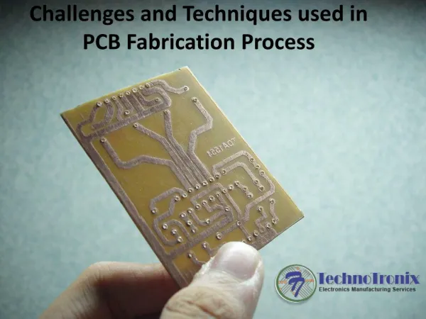
Challenges and Techniques Used in PCB Fabrication Process
80 likes | 262 Views
The demand of PCB fabrication service in USA has shown a remarkable growth in terms of quality of offerings and innovation. The business in user industries generated new orders in PCB fab in California . Thus current market trend is a fusion of various technologies for an error-free, optimal used resources and quick turnaround for the customers. More Information visit http://technotronix.us/pcb_fabrication.html

Challenges and Techniques Used in PCB Fabrication Process
E N D
Presentation Transcript
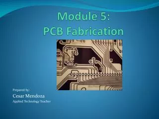
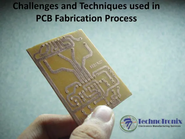
Challenges and Techniques used in PCB Fabrication Process
• A printed circuit board is a self contained model of electrical support to surface mounted and socketed components in the electrical devices. The significance and combination of design, fabrication and customer demand of Printed Circuit Board plays a vital role in developing an exact product as specified by the customer. A trend of complete turnkey has been adopted in the market conceptualization, design, surface mount or through- hole technique, assembling, testing and delivery of order to the customer. right from control
• There are international standards followed to maintain an assurance over quality as well as durability in the printed circuit board. This solely depends on the type and level of design created for a prototype. The challenges faced at the time of fabrication like inadequate fiducials ( reference point ) , polarity , hole size, tabs, proper paneling , dry parts, vias in pads, large deltas, thermal relief , leadless devices, close proximity of devices, trace cuts, proper finishing and clear laminate stack solely depends on the blueprint and the design of the prototype.
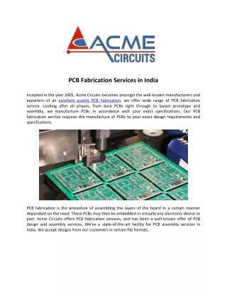
PCB fabrication process • Every product or prototype has a different layout as per the space allocation. There are special software to design the circuit model on the board. Raw materials are then arranged as per the volume of the production, the type of product and purpose of the product. According to the circuit pattern and model the quantity and quality of inputs are decided. This is a significant criterion to be considered to make the project a cost effective and qualitative one.
• One can move forward with the PCB fab process after proper planning , design and adequate availability of raw materials .There are different types of process used for different kinds of PCB’s like two –sided, one sided and multilayered . To get started with the fabrication process the glass fiber is rolled to a particular thickness as per the design. The substrate material is curved by passing it to an oven. After that the layering of the copper foil are placed as per the size of the board. With this the holes are drilled on the layers as per the design and layout.
• The copper is plated with the help of an additive or subtractive process. The inner layer core, copper foil and prepreg are combined together with vacuum, heat or pressure to laminate them thoroughly. This is when the PCB is to be fabricated with multi layers. The copper plating creates metallic base onto the holes and surface of the board. The outer layer is then coated with the same type of foil used in inner coating of the layers in circuit board. Tin plating is done to maintain the traces , pads and walls while operating onto the outer layer .
• The strip-etch-strip process is used to remove developed dry resist from the coatings where the tin plate is not affected. Solder mask technique is being applied to level the panel. The CNC machine is used to cut the boards in equal sizes as per the PCB design and layout. At last the boards are tested for its durability and raggedness.
• The fabrication process depends on the volume of orders and demand of the PCB assembly or fabrication services to make it a cost effective and qualitative one. There is a growing demand of innovative and strategic business models in dominant industries of USA. The demand of PCB fabrication service in USA has shown a remarkable growth in terms of quality of offerings and innovation. The business in user industries generated new orders in PCB fab in California . Thus current market trend is a fusion of various technologies for an error-free, optimal used resources and quick turnaround for the customers.