Download
1 / 12
120 likes | 146 Views
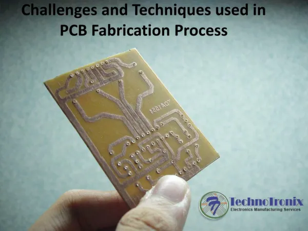
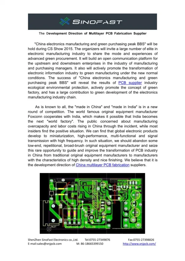
The smaller printed circuit board is often required in model making. Examples include eye switches for level crossings, power sources for car lights and others. The experienced model trainer may also want to tackle u201clargeru201d projects, such as his own booster with the desired performance. About PCB fabrication, it can be divided in different ways.<br>

E N D
5 Types Of PCB Fabrication The smaller printed circuit board is often required in model making. Examples include eye switches for level crossings, power sources for car lights and others. The experienced model trainer may also want to tackle “larger” projects, such as his own booster with the desired performance. About PCB fabrication, it can be divided in different ways. MOKO TECHNOLOGY https://www.mokotechnology.com/
Perforated plates and experimental plates The easiest way of PCB fabrication is with so-called experimental plates. These are PCBs made of hard paper or epoxy resin (GRP), which are drilled with a pitch of 2.54mm (= one-tenth of an inch). The copper layer is either just around these holes as pads or as strips. This means that smaller circuits can be set up quickly. The components are inserted on the side without copper and soldered on the other side. Connections can be made with thin wires and strands. However, this type of printed circuit board does not satisfy in the long run. It just looks too much like “handicrafts”. 1 3 4 https://www.mokotechnology.com/
Milling circuit boards Such a CNC router can possibly be made from a 3D printer yourself. The print head (the hot end) is replaced with a small milling machine.There are plenty of examples of how this works on the Internet. Most common 3D printers can be converted to CNC milling machines, such as RepRap, K8200, etc. Another option for PCB Fabrication Service is to take a copper-clad board and mill conductor tracks on it. A drill stand and a small, fast-running drill are sufficient. Corresponding conductor tracks can be milled freehand or with a stop using a small, pointed cutter. The holes for the components are then drilled. While this option is available for long, straight conductor tracks – such as passenger car lighting – the limit of what is possible is quickly reached with more complex PCB boards. In addition, it takes a lot of flair to mill paths freehand. This method can therefore only be used to a very limited extent unless you have a milling cutter with a motorized XY table. https://www.mokotechnology.com/
Etched circuit boards a The etched circuit boards are the simplest types of PCB fabrication. Material requirement • Bullet Copper-clad hard paper or GRP board (PCB raw material)• Bullet Waterproof felt tip pen• Bullet graph paper• Bullet etchants (iron-3-chloride, etch sulfate, aminiumpersulphate)• Bullet Lacquer• Bullet grains• Bullet Flat plastic tub•Bullet drill with small drills (0.8 / 1.0 / 1.2mm) https://www.mokotechnology.com/
Detailed PCB fabrication Process a First, you should draw a template. These are laid out on paper (preferably graph paper or tenths of an inch paper) and the connections marked, which later give the eyes. It can already be ensured that there will be no crossings of the conductor tracks if possible. Now it is time to connect the marked component connections. Inevitable crossings will later be made with wires on the component side, soldering eyes must also be provided for this. Now the etched circuit board is attached to the back of the template with tape, with the copper side to the paper. The markings on the connections are transferred onto the circuit board by hand using a punch with light pressure. https://www.mokotechnology.com/
Detailed PCB fabrication Process a Then, the conductor tracks can be drawn on the copper surface with the waterproof felt tip pen. Large copper surfaces should also be painted over if possible, this will make the etching process easier. After drying (at least 1 hour), the plate is placed in the approx. 1 cm high plastic tank filled with caustic. The etchant should have a temperature of approx. 35 – 50 ° C. Slightly “swiveling” supports the etching process. Remove the plate from the liquid and wash off with cold water. If you hold the circuit board in the light, any errors are immediately visible. https://www.mokotechnology.com/
Detailed PCB fabrication Process a Now the felt-tip pen color can be wiped off with household paper soaked in acetone or gasoline. To protect the copper and to facilitate soldering, the plate is sprayed with a thin layer of solder lacquer. After drying, the plate can be drilled – done! With a little practice, this circuit can be used to produce “worth seeing” circuits. But this technique is also subject to very narrow limits, especially due to the felt pen used (width of the line). In addition, this technique is hardly suitable for the series, since each plate has to be drawn individually by hand. https://www.mokotechnology.com/
Toner Transfer method a A better result than drawing on the copper surface with a felt pen is obtained with the toner transfer method. The template is printed in a mirror image on a carrier material with the laser printer and the toner is then transferred to the circuit board. The laser printer should produce a rich print image. Old, almost used toner cartridges should be replaced beforehand. Various coated papers (glossy surface) are suitable as the backing material, such as the backing paper for labels. Even better results can be achieved with a special toner transfer paper. https://www.mokotechnology.com/
Toner Transfer method a The actual transfer of the toner from the carrier to the copper layer takes place with heat. To do this, the paper is placed on the circuit board with the toner side and fixed with heat-resistant adhesive tape. Then press the iron on the paper at maximum speed for a few minutes. After cooling, the paper can be carefully peeled off, the toner now adheres to the copper. For optimal adhesion, it is necessary that the copper surface is cleaned well beforehand. Household sponges (such as Scotch Brite) with a rough surface and normal powder cleaner (e.g. Vim cleaning powder) and lukewarm water are suitable. With this method, quite precise circuit boards with thin tracks can be created. https://www.mokotechnology.com/
Toner Transfer method a As an alternative to transferring the toner with heat, the chemical transfer must also be mentioned here. To do this, the template is printed out in a mirror image on a sheet of a magazine (simply tear out one page and print the template over the text or images). Place this paper with the toner side on the circuit board and fix it with adhesive tape. Then coat the paper well with nail polish remover, rub it in again and again with your finger. The paper must be completely wetted. After the nail polish remover has dried, peel off the paper. Wash the circuit board with lukewarm water to remove any color residue from the magazines. With both methods, the circuit board can then be etched directly in the etchant as described above. https://www.mokotechnology.com/
Professional PCB Fabrication Service a All of these limitations lead us to the professional way of PCB fabrication, even if as a hobby electronics technician we use simpler means and tools. This method includes the following steps: Create Template Photographically transfer the template onto the circuit board Etch circuit board Drill Equip and solder https://www.mokotechnology.com/
Material requirement In addition to the previous version, the transfer of the template to the PCB fabrication is done photographically. The following material is required for production in this way: • bullet PC and printer• bullet graphic software, such as Corel Draw, AutoSketch or a special print layout software• bullet exposure lamp and glass pane or exposure case• bullet Flat plastic tubs (at least 2)• bullet drill with small drills (0.8 / 1.0 / 1.2mm)• bullet tracing paper or (special) carrier foils for print production• bullet Photo-coated PCB material (positive)•bullet Suitable developer liquid• bullet etchants (ferric chloride, etch sulfate, aminium persulfate)• bullet Lacquer MOKO TECHNOLOGY