SEMINAR ON LCD & FLAT PANEL DISPLAYS
440 likes | 779 Views
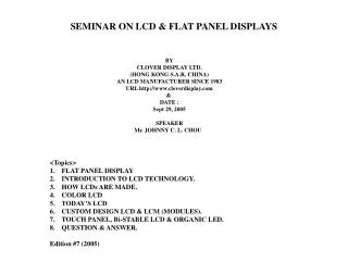
SEMINAR ON LCD & FLAT PANEL DISPLAYS. BY CLOVER DISPLAY LTD. (HONG KONG S.A.R, CHINA) AN LCD MANUFACTURER SINCE 1983 URL http://www.cloverdisplay.com & DATE : Sept 29, 2005 SPEAKER Mr. JOHNNY C. L. CHOU. <Topics> 1. FLAT PANEL DISPLAY

SEMINAR ON LCD & FLAT PANEL DISPLAYS
E N D
Presentation Transcript
SEMINAR ON LCD & FLAT PANEL DISPLAYS BY CLOVER DISPLAY LTD. (HONG KONG S.A.R, CHINA) AN LCD MANUFACTURER SINCE 1983 URL http://www.cloverdisplay.com & DATE : Sept 29, 2005 SPEAKER Mr. JOHNNY C. L. CHOU <Topics> 1. FLAT PANEL DISPLAY 2. INTRODUCTION TO LCD TECHNOLOGY. 3.HOW LCDs ARE MADE. 4. COLOR LCD 5. TODAY’S LCD 6.CUSTOM DESIGN LCD & LCM (MODULES). 7.TOUCH PANEL, Bi-STABLE LCD & ORGANIC LED. 8.QUESTION & ANSWER. Edition #7 (2005)
2.0. LIQUID CRYSTAL 2.1. Three major characteristics of Liquid Crystal 2.1.1. The Thermal Nature Solid State (Crystal) Liquid Crystaline State Liquid State Low Temp High Temp Melting Point Clearing Point 2.1.2. The Optical Nature of a LC molecule XXX NO light passing through Light Light passing through 2.1.3. The Electrical Nature of the LC molecules Electrodes AC potential No potential field P.2.
2.2. COMMON STRUCTURAL PHASES in the Liquid Crystal State Smectic Phase Nematic Phase Cholesteric phase 2.3. Two other components to make a Liquid Crystal Display Panel 2.3.1. Transparent Electrodes ---- Glass with conductive ITO layer which is etched to form a pattern. 2.3.2. The Polarizer Film Outgoing light & its axis Light wave & its axis Polarizer & its light axis P.3.
2.4. A TYPICAL TN TYPE LCD CELL Polarizer (Axis 0 degree) Glass with electrodes NO power supply With AC Volts connected Glass with electrodes Polarizer (Axis 90 degrees) Cell Gap = The separation between two glasses Positive Mode = Black digit on the grey background Negative Mode = Clear digits on the dark background Light P.4.
2.5. THREE COMMON TYPES OF LCD 2.5.1. TRANSMISSIVE TYPE LCD Light (Back Light) Eyes POLARIZERON BOTH SIDES 2.5.2. REFLECTIVE TYPE LCD Incident Light POLARIZER ON THE FRONT SIDE REFLECTOR ON THE BACK SIDE 2.5.3. TRANSFLECTIVE TYPE LCD Day Light Night Light (Back Light) POLARIZER ON THE FRONT SIDE TRANSFLECTOR ON THE BACK SIDE P.5.
2.6. CHARACTERISTIC CURVES Vs (Saturation Voltage) % LIGHT ABSORPTION (or TRANSMISSION) Vth of LC 90% changes At higher Temp. 5 v 4 v 10% change VOLTS 0 volt -40 deg C +80 deg C Vth (Threshold Voltage) LC Fluid Viscosity % Light Absorption mm2/sec 10,000 At a lower Temp. 100 Time Toff 20ms to 300ms Ton 5ms to 100ms -40 deg C +80 deg C Depending on how the LCD fluid is formulated. The smaller the cell gap, the faster response. P.6.
2.7. TN & STN (Super Twisted Nematic) The LC molecule mid-plane tilt angle Vth Vs % Light Absorption % Light Absorption % Light Absorption 90 deg Twisted 240 deg 180 deg Twisted Twisted Volts V 0 V 0 0 Wide View Angle Narrow View Angle TN LCD STN LCD Yellow Green background color In the positive mode Grey Background in the positive mode P.7.
2.8. HTN (Highly Twisted Nematic) & FSTN (Film STN) STN 180 deg or higher deg Twisted TN 90 deg Twisted Wide View Angle BUT with Darker Color Background & Blue or dark blue patterns. Narrow View Angle HTN 110 deg Twisted FSTN 240 deg or higher deg Twisted 1st Minimum TN Little wider View Angle than TN (see later pages) Wider View Angle than TN but narrower than STN View angle same as 240 deg STN BUT in Grey Background Color & Black patterns. Polarizer DSTN (Double STN Cells) 1st Cell with patterns Same as usual STN Old way when NO Retardation film LCD Cell 2nd Cell without pattern But in reverse twisting Retardation Films on Polarizers to correct the color phase P.8.
2.9. COMPARISON AMONG TN, HTN, STN & FSTN 2.9.1. Positive Mode (Pattern on a Clear Background) P.9.
2.9.2. Negative Mode (Clear Pattern on a Color Background) Other natures same as the Positive Mode. 2.10. Gooch-Tarry Curve --- The 1st Minimum TN LCD % Transmission n : Birefringence (reflective indices of Light transmitted in parallel & perpendicular To the director of LC molecules. 12% d : the cell gap 8% 4% 0% d n 0.48 (1st Min* ) 1.05 (2nd Min) 1.64 (3rd Min) (um) P.10. *The 1st Min process is patented by E. Merck.
2.11. THE STATIC & MULTIPLEX DESIGN OF ELECTRODES 4 pairs of electrodes 8 connectors needed. No time sharing for the input signals – The STATIC Design 4 electrodes in matrix 4 connectors needed. 1/2 time sharing for the input signals to both the top and bottom electrodes---- The MULTIPLEX Design. We call it 1/2 duty if the 1/2 time sharing is used on the Common. 5 electrodes 5 connectors needed. 1/4 time sharing for the input signals to each of the top electrode. No time sharing for the bottom glass. We call the top electrodes the SEGMENT while the bottom electrodes the COMMON. PROBLEM: The higher the duty ratio, the shorter time the power signal goes into each electrode pair. Finally the power rms value may NOT be enough to fully drive the LC twisting properly. P.11.
2.12. THE PASSIVE AND ACTIVE LCD Y1 Y2 Signal X1 Time X2 Signal An ACTIVE Component ; MIM (metal insulator metal) Diode Or TFT (thin film transistor) Time The LCD Pixel The TFT method is commonly used today on the large DOT MATRIX LCD, we call it the ACTIVE MATRIX LCD, or AMLCD The LCD built together with the Active Component is not only the TFT LCD. The LCOS is also an LCD built on a silicon wafer with active components to control the LCD. In general, the duty ratio over 1/256 may not give a good contrast in the Passive design. But there are still some special design to work in the Passive way, such as; Dual Scan STN (DSTN), High Performance Addressing (HPA), …. etc P.12.
2.13. THE HISTORY OF LC & LCD Application Approx Year Major Development Liquid Crystalline initially described by an Austrian Scientist, Mr. Friedrich Reinitzer. 1888 1904 E. Merck sold the first Liquid Crystal substrates to the research market. 1960 Westinghouse used the cholesteric LC as a temperature indicator. Thermometer 1965 RCA demonstrated a dynamic scattering LCD to show numeric symbols. Kent State Univ. in Ohio USA presented an LCD operated at room temp. 1970 Rockwell (USA) and Sharp (Japan) made LCD Calculators. Hull Univ. in England synthesised new biphenyls with excellent physical properties for display use. Higher Contrast Twisted Nematic Mode in use. OCLI (USA) coated ITO on glass as electrodes. BDH (UK) sold LC to LCD manufacturers. Calculator Time pieces 1975 Hamlin Inc (USA) in TN LCD mass production. E. Merck introduced Biphenylcyclohexanes LC for higher multiplex. Instruments Motorola built LCD on 4 ½”x 4 ½” glass substrates Microma (USA) further improved the mass production technique and Fairchild Semiconductor Inc. moved LCD production to Hong Kong. Timex (USA) bought RCA LCD facility and merged with Fairchild. The Japanese developed a Chemical Sealing process for cost reduction. Data bank & PDA P.13.
2.13. THE HISTORY (continued) Application Approx Year Major Development The first LCD scriber made by Villa Precision Inc. (USA) Roche, BDH, E.Merck improve LC mixtures for TN, STN 1980 5x7 Character Dot Matrix Graphic Word Processor Fairchild scaled up to 14x14” substrates Clover Display Ltd established in May 1983 MIM & TFT AMLCD invented Full Dot Matrix & TV Panels Brewer Science Inc. & OIS of Troy, USA developed colour AMLCD for space shuttle use. 1985 PDA, Laptop & Notebook PC Full color TFT panel for Notebook PC 1990 Mobile phones 1995 Bi-stable Cholesteric LCD E Books 2000 New Display to replace LCD ?---- OLED, PLED P.14.
3.0. HOW LCDs ARE MADE 3.1. THE FRONT END PROCESS ITO = Indium Tin Oxide, a transparent conductive layer coated on the Sodium Lime Glass. Its resistance is from 10 Ohms to 120 Ohms/square. Glass area usually in 14x16”. Thickness in 1.1, 0.7, 0.5, 0.4, 0.3mm ITO Glass Clean Glass with DI water Artwork & Mask Design Methods: Photo Masking, Resist Ink Printing, ITO Ink direct Printing, Laser Cutting. Patterning the Electrodes on ITO Alignment Layer To form a rough surface to hold the LC molecule chains To form the cell and the inter-connections between the top and bottom glasses Sealing Frame & Silver Dot Printing Top/bottom Glass Alignment and Seal The Laminated pairs P.15.
3.2. THE BACK END PROCESS Laminated Pair Cutting into cells Liquid Crystal Mixture Formulation Liquid Crystal Filling End Sealing & Cleaning Testing & Inspection Polarizer Cutting Polarizer Fixing Metal Pin or Heat Seal Connector fixing Cosmetic Check LCD Module Assembly (COB, TAB, COG, COF) Optional Process Shipments P.16.
4.0. THE COLOR LCD 4.1. THE FULL COLOR LCD Black and White LCD Full Color LCD Slice ITO into narrow sections Segments RGB Color Filter Common Common In order to give a better color mixing, the RGB line widths are usually less than 30 micron in width per color. Hence the same for the ITO electrodes. The color LCD can be built as a Passive LCD. But most large size Dot Matrix Color LCDs are built in the Active design. P.17.
4.0. THE COLOR LCD (continued) 4.2. THE ECB (ELECTRICALLY CONTROLLED BIREFRINGENCE) COLOR LCD % Light Absorption Various ECB Types; 1) Homogeneous Type Red->Yellow->Green->Blue 2) Deformation of Vert Aligned Plane (DAP) Type Blue->Green->Yellow->Red 3) Hybrid Aligned Nematic (HAN) Type Green->Red->Blue 4) Vertical Aligned Nematic (VAN) Type 0 V Clear Dark Grey Y O R P B G Color around 2.4v to 3.7v Dark V No pure color, 50% Green + 25% Red + 25% Blue at this point P.18.
4.3. DOUBLE CELL COLOR LCD There are two kinds of double cell can generate colors; A) With Color Polarizer B) With usual Polarizers at certain angles (Only working in Transmissive Mode) (Reflective Mode is also possible) 4.4. GUEST HOST LCD (Single fixed color) Mixing color dye in the LC fluid and build LCD in Negative Mode. It will show clear pattern on a color background. Such method was used in the early date. 4.5. LCD WITH COLOR POLARIZER, COLOR FILM OR COLOR REFLECTOR IN CERTAIN AREA (fixed color) Pre-printed color polarizer is expensive. 4.6. COLOR INK PRINTING ON THE BOTTOM GLASS SURFACE (fixed color) This is the cheapest way to make LCD with fixed colors. The LC image & color area may not coincide well due to the glass thickness. P.19.
5.0. TODAY’S LCD Active LCD Duty Ratio LCD TV & Monitors Passive LCD 1/256 Projector Portable TV Notebook Panels 1/128 1M+ Pixels Digital Camera Office Equipment 1/64 PDA 100K Pixels 1/32 Mobile Phone Digital Instruments STN 1/16 TN 10K Pixels Data Bank 1/8 1/4 1K Pixels Film Camera Calculator 1/3 100 Pixels 1/2 Time pieces Hand Held Games Panel Size 1/1 Static 10,000 10 mm2 100 1,000 100,000 mm2 P.20.
6.0. CUSTOM DESIGN LCD & LCM --- The factors to consider 6.1. LCD PANEL DIMENSIONS Outer Dimensions (Be economical size) View Area (normally 2mm from the edges) End Seal (0.5mm thick) Active Area (Area with patterns) Pinout or Connection Area (2 to 2.5mm) Glass Thickness (1.1, 0.7, 0.5, 0.4 or 0.3mm/one side) ( Glass Material: Sodium Lime Glass with SiO2 barrier, surface polished for STN use ) Economical Panel Size: The outer dimension may use up most the raw glass sheet area. For small order size or pilot run, 7x8 inches sheets are used to boost up the yield and save the tool cost. or Raw Glass Sheet 7x8 inches (178x203mm) 14x16 inches (355x406 mm) (The usable area is 7mm off the edge) P.21.
6.2. PANEL CONFIGURATIONS The thick lines representing the pinout areas. A B C D Connectors suitable: Zebra (Silicone Rubber) – A, B, Heat Seal or TAB – A, B, C, D, Metal Pins – C, D, Eyes All the above 4 models required Ag (silver) connections inside the LCD cell. If such Ag connection not to be used or unable to be used, the configurations will be as follows; G E F Models E, F & G are good for combination use of Zebra and Heat Seal connectors together. Most TAB connections are also applying on such models. 40+deg 40+deg 15+deg For TN LCD, don’t forget to specify the View Direction 45+deg 45+deg 15+deg 6 O’clock P.22. 12 O’clock
6.3. PATTERN LAYOUT Too Long Trace Cross Over Narrow down trace Good Layout Bad Layout C S1 S2 S3 S4 S5 S6 S6 S3 C S1 S2 S4 S5 + P.23.
6.4. ZEBRA CONNECTORS Three kinds of Rubber 1. Sponge Rubber 2. Silicon Rubber 3. Super Soft Rubber Side Wall Insulators Conductive Layers Insulation Layers Metal Mounting Bezel Pitch: (Conductor/Insulator Layers) LCD Assembly Low Cost Type --- 0.25+-0.05mm General Type ----- 0.18+-0.04 mm Dot Matrix Type – 0.10+-0.03 mm Graphic Type ------0.05+-0.025 mm Zebra PCB Contact Resistance: 1000 –1500 ohms at 10%-15% compression Precautions in Assembly • Pre-clean Zebra • Three or more conductors in contact • PCB wraping <0.375mm / 50 mm • Bezel has opening gaps with PCB • 0.3mm or 10%-15% compression • Dummy zebra use with single side • contact LCD. • Insulation side wall quality. LCD Zebra Good Mis-aligned A safer way (wider contact on PCB) P.24.
6.5. HEAT SEAL CONNECTORS Conductors (~20 um particles) printed on a Polyester (PET) Film of 20 -25um Contact Resistance & Pitch Graphite Type --- 35 to 100 ohms/sq 0.40, 0.60, 2.80 mm Silver Graphite Type ---- 0.5 ohm/sq 0.23, 0.35, 2.80 mm Silver Type ------ 0.05 ohm/sq 0.23 mm Hot Press Choose proper LCD configuration: PET film LCD Conductor side Welded PET side PCB Precautions in Assembly PCB • The Hot Press head temperature 120-140 deg C at joint • 32 Kg/sq cm pressure is recommended • Leveling the press for even pressure along the joint. • Properly select the sealing time to prevent uneven flow or • wash away the conductor particles. • 100pcs/mm2 particles at contact area is suggested. • Peeling off strength be >200gm (Vertical) • & >500gm (Horizontal) PET side LCD PCB PET side P.25.
6.6. METAL PIN CONNECTORS ( for 0.7 & 1.1mm glass ) Standard Pitch: 1.27mm, 1.8mm, 2.0mm, 2.54mm Pin Length: 20mm, 30mm, & 45mm max LCD Clip Depth 2.0mm to 2.4mm max Contact Resistance: <0.05 ohm • Precautions in Assembly: • Prolong soldering may damage the Pin contact to glass • ---- A good LCD will add carbon cushion between pin • clip and glass contact area. • Care on bending the pins ---- LCD maker provides pin • lead forming. • Pin length under 4.0mm is not recommended. • Wave solder is not recommended ---- Polarizer is weak • Mechanical stress on pin or temperature changes may • cause LCD background color changed. Epoxy enforcement Wider seal area is required. All the above connections may have IC on PCB by SMT, Wire Bonding (COB) or Insert & Solder. 6.7. TAB (TCP IC BONDING) LCD IC on a flexible film with conductors. The Film is heat sealed onto the LCD pinout area TAB = Tape Automation Bonding TCP = Tape Carrier Package P.26.
6.8. CHIP ON FILM (COF) LCD Same as TAB, but with more components on the film like a circuitry on PCB 6.9. CHIP ON GLASS (COG) The IC Chip for COG is different from those for usual wire bonding on PCB. Same as an usual LCD LCD Glass with Fine traces Fan-in & Fan-out ACF* film is used to fix the COG chip onto the glass. The ACF film is similar to Heat Seal but with much finer Pitch and conductive particles. Most panels with Metal Pins IC Chip * ACF=Anisotropic Conductive Film P.27.
6.10. TRICKS ON THE LCD PANEL DESIGN Recommended Driving Freq 60 Hz to 120 Hz 6.10.1. THE BIAS VOLTAGE Theoretical Driving Waveform % LIGHT ABSORPTION Applied to Segment 90% Applied to Common 10% Resulting Waveform to LCD Volts 0 volt Vth Volts Off On Practical Design Waveform (Example: Waveform to LCD at 1/3 Bias) V On 2/3V Off Off 1/3V The Bias Voltage The driving Voltage 0 -1/3V -2/3V Time -V P.28.
6.10.1. THE BIAS VOLTAGE (continued) The formula and design facts; N: Multiplex Rate. Example: N=3 for 1/3 duty S: Bias The ideal design S=1+ N Vd: The supply voltage to the panel. Von = ( Vd / S ) x ( N-1+S ) / N Voff = ( Vd / S ) x [ N – 1 + ( S – 2 ) ] / N 2 2 Less than 1 volt ! Beware the drifting under temp changes P.29.
6.10.2. CROSS OVER LAYOUT Epoxy Sealing Frame S1 S2 S3 S4 C1 Ag Dot Connection Hided under Frame C2 C1 2 cross over points 6.10.3. THE POLARIZER SELECTION • The Glue Type or Non-glue Type polarizer. • The Polarizer with the UV Barrier may extend the LCD Life under strong UV exposure. • The Anti Glare Polarizer may improve the contrast. • The high durability polarizer may stand for wider temperature environment. • The slightly orientation of Polarizer axis may change the background color. 6.11. THE THERMAL COMPENSATION It is recommended to use the thermal compensation circuit when a LCD will be operated under a wide temperature range. P.30.
6.12. TEMPERATURE RANGE Wide Temp Type Clearing point Melting point Low Temp Type General purpose Temp Deg C Operating Temp. -30 0 deg +75 deg -20 +50 +60 Storage Temp 10 deg C lower 10 deg C higher The STN temp is 10 deg narrower than TN Background blackened Cross Talk Problem when exceeds rated temp. Black Spots Slow response All the above defects are reversible at room temp Possible design Specific for High Temp Specific for Low Temp Temp +100 +10 +30 deg -40 deg P.31.
6.13. BACK LIGHTS Important: The Transmissive and the Transflective Type LCD absorb the different light intensity. Light Light - Diffuser Paper Light Guide LED wiring LEDs + Reflector domes Fig. 1. Reflector Paper Fig. 2. P. 32.
7.0. BI-STABLE LCD Bi-stable Cholesteric Display, or SSCT – Surface Stabilised Cholestric Texture Display, or Multi-stable Chiral Nematic Display, or E-Book Display • This is a new technology in LCD making use of the Cholesteric Liquid Crystal. Mr. John West • and Mr. D. K. Yang of Kent State University, Ohio, USA filed the patent in 1995. • The display image is retentive in the absence of an electric field. It has a excellent readability • and wide view angle under the daylight or strong ambient light. • No Polarizer is required on this kind of display panels. • The Liquid Crystal is switchable and stable in two kinds of texture. • The Twisted Planar Texture, which has the LC layers parallel to the display surface, • reflects the incident light. • (b) The Focal Conic Texture, whose LC is in fragmentary, scatters the incident light. Switch-able (a) (b) The above two textures are switch-able under 30V to 180V pulse of 10ms to 100ms, and stable in zero electric field. By properly adjust the pitch of the Twisted Planar Texture, it can reflect R, G, B lights. P.33.
8.0. ORGANIC LED The Organic Electro Luminescent Displays (OELD) , or The Organic Light Emitting Devices (OLED) The EL ( Electro-luminescence ) Back Light for LCD has been used for many years. It operates at high voltage (>100V). In 1987, Tang and Van Slyke in Kodak, USA reported a low voltage (<10V) Organic EL. It comes a new display ---- the OELD. 8.1. THE BASIC STRUCTURE Metal Cathode Electron Transport Layer DC volt Re-combination and Emission Layer Hole Transport Layer ITO Layer (Anode) Glass Substrate Light emits 8.2. THE DIFFERENCE BETWEEN LCD & OLED LCD OLED No Light emission Emits light in colours (100cd/sqm) Narrow view angle Wide view angle (>150 degrees) Slow response Fast response (<10 microsec) OLED has most the advantage of LCD such as; Easy patterning Low operating voltage but at high current ( 20ma/cm2) Low manufacturing cost Thin and light weight P.34.
8.0. ORGANIC LED (continued) 8.3. THE OLED & PLED • There are two major ways to build the OLED; • The small molecule process ---- by spluttering the organic materials onto the ITO patterns. • Kodak uses such way. • The large molecule process, or the polymer process ---- by spin coating, dip coating or screen • printing the organic pastes layer by layer. Cavendish Lab in Cambridge, UK and Dow • Corning, USA developed such process and materials in ’90s. • Some people now call the OLED made under polymer process the PLED. • The small molecule process is also applying to making the ACTIVE OLED. • Pioneer, Japan seems the first one in mass production for the OLED. • It is expected the OLED will replace the LCD step by step from 2005. • CLOVER DISPLAY GROUP has started a joint venture with the University of Hong Kong to research • and develop the materials and process for OLED. • The newly formed joint venture company is named COLED DISPLAY LTD., established Sept 2002. P.35.
9.0. TOUCH PANELS PE Film With ITO 9.1. ANALOG TYPE Ra Rb Silver Conductors A PE film with ITO layer is sealed onto an ITO Glass with epoxy dots as Spacer to maintain a gap. When the external pressure of touching makes contact of two ITO layers, the sensing IC circuit with give an analog reading corresponding to the touch position. Epoxy dots As Spacer Rd Glass with ITO Pin out Area Rc 9.2. DIGITAL TYPE The ITO on the PE Film and the ITO Glass are etched out into sectors. When touched, the corresponding sectors are shorted circuit and reflected to the pins concerned. PE Film With ITO Epoxy dots As Spacer Glass with ITO Pin out Area P.36.
10.0. CUSTOM LCD/LCM DEVELOPMENT GUIDE. Enquiry from Customer Feasibility Study & NRE Charge / Unit Price Quoted Free quote in 2-4 working days NRE payment in advance NRE Order Confirmation ** normally 10-20 LCD or 3-5 LCM samples will be free. For more qty, please notice us in advance when confirm the NRE order. LCD Panel PCB & Circuit External Casing 1 week 1 week 1-3 weeks Panel Drawing for Approval Circuit diagram & PCB Layout Case Drawing 3-6 weeks 3-4 weeks 3-10 weeks Mask Design & Samples** for Approval PCB Tool Design & Samples** for Approval Hand mould up sample Final Case Mould 3-9 weeks Primary Sample Final Sample Total development time; LCD Panels 4-7 weeks, LCM Modules 4-10 weeks; With External Case 7-18 weeks P.37.
11.0. ACKNOWLEDGEMENT & DECLAIMER We have tried our best to present up-to-date and correct information here. Some of them to be explained together with photographs and demonstration samples to form a complete part of the Introduction. We wish that the information discussed in this seminar may help the design engineers to make a cost effective and quality custom design in an easier and logical way. However, this is not an academic seminar that we have used a simply way in the presentation. All information here is provided in good faith without any expressed or implied warranty. The reader should seek for more detail advice from the industry. • The information in above are partly referring to the following documents; • Proceedings of the Liquid Crystal Seminar HK by E. Merck, Darmstadt, Germany. • Various articles in the SID International Symposium and Information Display by the Society for • Information Display, Inc. USA • LCD Displays, the leading edge in flat panel displays, by Sharp Technical Library, Vol. 1, of • Sharp Corporation, Osaka, Japan. Editions: 7th edition Sept 29, 2005 6th edition Mar 13, 2003. 5th edition Sept 19, 2001. 4th edition Apr 16, 2000. 3rd edition Sept 6, 1999. 2nd edition Sept 1, 1998. 1st edition May 19,1997. All copy rights reserved Clover Display Ltd. H.K. Prepared by; Johnny C. L. Chou, Clover Display Ltd. Room 1006, 26 Hung To Road, 10/F, Kwun Tong, Hong Kong Tel: 23428228, 23413238 Fax: 23418785, 23574237 email: cdl@cloverdisplay,com URL: http://www.cloverdisplay.com (in English) http://www.cloverdisplay.com.hk (in Japanese) http://www.cloverchina.com (in Chinese) P.38.