Download
1 / 12
120 likes | 304 Views
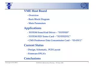
VME Host Board - Overview - Basic Block Diagram - Main Parameters Applications - TOTEM Frond End Driver – “TOTFED” - TOTEM FED Tester Card – “TOTFEDTC” - CMS Preshower Data Concentrator Card – “ES-DCC” Current Status

E N D
VME Host Board • - Overview • - Basic Block Diagram • - Main Parameters • Applications • - TOTEM Frond End Driver – “TOTFED” • - TOTEM FED Tester Card – “TOTFEDTC” • - CMS Preshower Data Concentrator Card – “ES-DCC” • Current Status • - Design, Schematic, PCB Layout • - Firmware FPGA’s • Conclusions
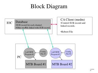
VME Host Board (1) Overview General Requirements are: - Two different applications – TOTEM and CMS Preshower; - Different Data Density – TOTEM not need to concentrate data; (bit/channel/event), CMS ES need to reduce data (N-bits/channel/event) - VME interface (CMS) with possibilities of stand alone mode (USB). Selected Implementation: - Standard VME64x 9U Board with Mezzanines Cards; - Mezzanines Cards: “OptoRX” – 12ch Optical Receiver; “S-Link64” – standard CMS S-Link64 board; “VFAT Emulator” – 12 channels Optical Transmitter VFAT emulator; “DRM” – Data Reduction Module; - Upgrades Capabilities – modular design.
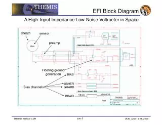
OpRX 1 + S-Link64 VME64x Interface MAIN 1 USB 1 Spy 1 Memory JTAG VME64x OpRX 1 + S-Link64 Local Bus MAIN 2 DRM USB 2 Spy 2 Memory To S-Link64 OpRX 1 + S-Link64 MAIN 3 USB 3 CCS/TTS Spy 3 Memory Optional Local Bus CLOCK TTCrx QPLL CLOCK VME Host Board (2) Basic Block Diagram
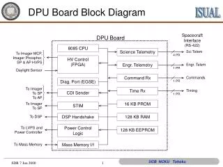
Spy 4 Memory 192bits 64bits OpRX 1 + S-Link64 32bits VME64x Interface 32bits MAIN 1 16bits USB 1 Spy 1 Memory JTAG VME64x OpRX 1 + S-Link64 Local Bus 32bits MAIN 2 Merger FPGA 16bits USB 2 Buffers Spy 2 Memory 64bits OpRX 1 + S-Link64 To S-Link64 32bits MAIN 3 16bits USB 3 CCS/TTS Spy 3 Memory Local Bus Optional 16bits CLOCK USB 4 TTCrx QPLL CLOCK VME Host Board (3) Basic Block Diagram
VME Host Board (3) Main Parameters • 9U VME64x Slave; • Local Bus Master 32bits/40MHz; • 18MB Spy Memory: • 3x of 6MB per 12 optical channels (1 OptoRX); • 96bits at 80MHz; • 3x Memory Controller; • 3x USB 2.0 Interface; • Merger + Memory; • TTCrx, QPLL and CCS clocks (optical or electrical); • TTS copper link; • JTAG controller on board; • Connectors for: • 3x OptoRX; • 1x DRM; • 3x S-Link64 + 1x S-Link64 on rear at 200MB/s • Board Temp. Measure
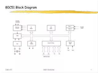
OptoRX OptoRX OptoRX S-Link S-Link S-Link VME Host Board Applications (1) TOTEM Front End Driver – “TOTFED” “TOTFED” is a set of: - 1x VME Host Board; - 3x OptoRX Boards; - 3x S-Link64; Firmware: - Slow Readout VME or USB; - Event Builder in OptoRX FPGA; - S-Link64 to CMS DAQ.
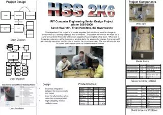
OptoRX VFAT Emulator S-Link VME Host Board Applications (2) TOTEM FED Tester Card – “TOTFEDTC” “TOTFEDTC” is a set of: - 1x VME Host Board; - 1x VFAT Emulator (see EDMS); - 1x OptoRX; - 1x S-Link64. Firmware: - Data from VME or USB; - Event Builder in Main FPGA; - Data Read Back.
OptoRX OptoRX S-Link OptoRX DRM VME Host Board Applications (3) CMS Preshower Data Concentrator Card – “ES-DCC” “ES-DCC” is a set of: - 1x VME Host Board; - 3x OptoRX Boards; - 1x DRM; - 1x S-Link64 – back. Firmware: - Slow Readout VME or USB; - Event Builder in DRM FPGA; - S-Link64 to CMS DAQ.
Current Status (1) • Design • Defined together with CMS Preshower people to • satisfy both groups requirements; • Based on experience from other similar designs. • Schematic (see PDF) • - Done with Cadence CERN; • - Finished 27 pages A3; • - Next in EDMS.
Current Status (2) • PCB Layout • Pending; • Job in DEM started; • Layout min 4 weeks; • See Preliminary • placement --->>>
Current Status (3) Firmware FPGA’s • VME64x Interface Controller: • - ALTERA Cyclone EP1C4F400 • - Futures: • - VME64x Slave A32/D32; • - Block Transfer; • - Bridge and Local Bus Master; • - JTAG control. • - MAIN Controller: • - ALTERA Stratix EP1S20F780 • - Futures: • - 6MB ZBT SRAM Memory Controller; • - 192 bits SPY Data Input; • - Switch between Local Bus, SPY Data Input and USB Output; • - USN 2.0 controller.
Conclusions • VME Host Board is a complex design; • Need to cover several different requirements; • It is based on modular principle, therefore: • It is easy to develop and test separate mezzanines; • Build unit not fully equipped (cost, performance); • Easy to Upgrade, replace/redesign mezzanines. • Issues; • Interconnectivities, Connectors and Plug-in; • Need First Prototype and Firmware to verify.