A scalable DAQ system using the DRS4 sampling chip
200 likes | 439 Views
A scalable DAQ system using the DRS4 sampling chip. H.Friederich 1 , G.Davatz 1 , U.Hartmann 2 , A.Howard 1 , H.Meyer 1 , D.Murer 1 , S.Ritt 2 , N.Schlumpf 2 1 ETH Zurich, Switzerland 2 Paul Scherrer Institute, Switzerland. Outline. 1. Introduction WaveDREAM Project DRS4 Chip

A scalable DAQ system using the DRS4 sampling chip
E N D
Presentation Transcript
A scalable DAQ system using the DRS4 sampling chip H.Friederich1, G.Davatz1, U.Hartmann2, A.Howard1, H.Meyer1, D.Murer1, S.Ritt2, N.Schlumpf2 1 ETH Zurich, Switzerland 2 Paul Scherrer Institute, Switzerland
Outline 1. Introduction • WaveDREAM Project • DRS4 Chip 2. Realization • Analog Frontend • Continuous Digitization • Digital Backend 3. Results • System Bandwidth • Noise Power Spectrum • System Nonlinearity
WaveDREAM Project • Motivation: 1 GSPS, 8-bit, low cost, multichannel system for pulse shape discrimination and photon counting • Development of a flexible DAQ system • Based on the DRS4 chip • Active amplification • 20 dB gain • ≥ 500 MHz bandwidth • Scalable no. of channels • Optimized for small amplitude (~10 mV), high frequency signals (~1 GHz), e.g. PMT • Capability for 1 ns global event timestamps • Digital Trigger (FPGA) • General purpose board
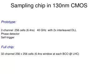
DRS4 Chip (Developed at PSI) • Large Switched Capacitor Array (SCA) • Stores the analog waveform • up to 5 GSPS • 11.5 bit SNR • Slower SCA readout • Less expensive ADC electronics • Region of interest readout • NumberOfBins x 30 ns • 8+1 channels • Individual Channel depth 1024 bins • Channel cascading • Parallel or serial channel readout
DRS4 Transparent Mode • Input directly accessible at output while recording • 50 MHz Bandwidth • Continuous sampling of the input • Same ADC as DRS readout • Digital trigger • Arbitrary event record length • Eliminates the need for splitting the signal at the frontend • Reduces PCB complexity Transparent Mode gain: ½ of SCA gain MUX LP SCA
Design Realization Digital Trigger in the FPGA (e.g. Threshold, CFD) Board-to-board communication DRS4 ADC FPGA Gigabit Ethernet Analog Frontend UDP connection to backend Board-to-board communication Readout of all 8 pipelines in parallel Minimizes DRS4 dead time
Analog Frontend baseline DC offset DAC • AC coupled input • Fixed gain 20 dB • Adjustable baseline • Accommodates all signal polarities • Input remains in linear range of DRS4 • Frontend-only bandwidth > 1 GHz 50 50 DRS4 THS 4508 THS 4302 50 + 14 dB + 6 dB Input span: 1 V p-p Input levels between 0.1 and 1.5 V
Continuous Digitization AD9212 • Sample Modes: • Continuous • sampling • (120 MSPS) • DRS Readout • (30 MSPS) • AD9212: 8 Channel, 10 bit ADC, 65 MSPS • Transparent Mode: 50 MHz bandwidth • Sampling theorem: ≥ 100 MSPS or additional low-pass filtering • More bandwidth increases SNR for high-frequency pulses • Solution: 2 AD9212 with 180 degrees clock phase shift, 120 MSPS DRS4 FPGA CLK AD9212 Trigger
Global Timestamps • Global Clock & Reference signal distributed to all boards • Avoids clock skew • Use clock conditioner chips to reduce clock jitter • Sample the reference signal in the DRS4 to extract fine-grain timestamps • Calibrate propagation delays • Not tested – No numbers DRS4 FPGA LP
Prototype Implementation • Mezzanine Card • Analog electronics, DRS4 chip, ADCs • Carrier Card • Slots for 2 mezzanine cards • 2 FPGAs (Xilinx Spartan 3A) • Communication Layer • Gigabit Ethernet • UDP / IP / MAC layer in VHDL • Board-to-board communication • 960 Mbit/s • USB 2.0 • RS-485 • VME form factor (6U) • Provides mechanical support, power supply & cooling • No support for VME bus
Results: System Bandwidth • Input capacitance of DRS limits bandwidth • 500 MHz Bandwidth • Nonlinear amplification around 300 MHz
Transparent Mode Bandwidth Bandwidth [-3dB]: 60 MHz
Noise Power Spectral Density DRS Readout (1.024 GSPS) • ENOB 8 – 8.5 bit
Baseline Adjustment • Baseline can be adjusted • Linear adjustment circuit ADC range [0 1024]
Amplitude Nonlinearity • Amplitude Nonlinearity less than 1 ADC value
Applications • A performant system has been demonstrated • Possible applications include • Pulse shape discrimination • Photon counting from PMTs • Oscilloscope functionality • Arbitrarily flexible trigger logic in the digital domain • Window coincidence already implemented • If you’re interested in using the WaveDREAM board, please contact me afterwards
PMT Signals First part of transparent mode signal equals DRS readout signal
Conclusion • A challenging design realized • Good bandwidth achieved (500 MHz) • Region of interest sampling up to 5 GSPS • 120 MSPS continuous sampling • Digital Trigger logic • ENOB 8 - 8.5 bit • Gigabit Ethernet • Cost Effective • Flexible design for multiple applications • Thanks to Arktis Radiation Detectors Ltd & CTI for financial support