Download
1 / 16
160 likes | 176 Views
XFEL 2D Pixel Clock and Control System. XFEL Meeting, RAL 20 January 2011 Erdem Motuk, Martin Postranecky, Matt Warren, Matthew Wing. OUTLINE. Progress up to date Hardware Structure Firmware structure Current Status Outstanding Issues Future plans. Progress up to date.

E N D
XFEL 2D Pixel Clock and Control System XFEL Meeting, RAL 20 January 2011 Erdem Motuk, Martin Postranecky, Matt Warren, Matthew Wing
OUTLINE • Progress up to date • Hardware Structure • Firmware structure • Current Status • Outstanding Issues • Future plans
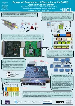
Progress up to date • Acquired software and licence for Allegro ConceptHDL • Design flow established – The first run slightly slow – improved for others • Schematic design and packaging at UCL – Layout at RAL • Test card A design • Schematic entry/layout finished – Named PC3461M • In the manufacturing and assembly stage • RTM design has started • Schematic entry started • xTCA crate has been purchased • Set up and running with SLC
Progress up to date • Firmware design on the development platform • Telegram transmit/receive • FAST message transmit/receive • Test Bench • Firmware comprising all transmit/receive blocks • Transmit can be started by external input (push-button or ChipScope VIO) • Results can be observed by ChipScope • PCIe • Development card can be accessed through PCIe • Manual start/stop (standalone operation)
Hardware Structure • PCM3461 Assembly drawing top and bottom sides Test / Prototyping area TRANSMIT RECEIVE
Hardware Structure • PC3461M to be used for • FAST message transmit/receive testing (via ETH cables) • Telegram message transmit/receive testing • Available for others to use (with the XUPV5 development board)
Hardware Structure RJ45 CONNECTORS (8/16) LVDS DRIVERS CLOCK / PLL I2C / EEPROM LVDS RECEIVE POWER • Prototype RTM to test with the DAMC2 board in the xTCA crate • Early prototype availability for the system • Diagnosing bugs/gotchas with the design • Later revision to add more capability • Prototyping platform • for extra features if needed • Tests to be carried out • in the actual setup (xTCA crate)
Firmware Structure • A test firmware that integrates transmit/receive and other features • One bit file to program the FPGAs on the dev boards • ChipScope cores associated with each block • Firmware diagram – Finished blocks + extras for test Clocking implemented according to the dev board Buttons on dev board Fast Message Receive implemented as a part of LPD FEM firmware Telegram transmit implemented for TR
Firmware Structure • Telegram transmit/receive • Two packet structures for data and events • Start Byte (x2C) + Write_Type + CRC (for events) • Start Byte (x2C) + Write_Type + Data (32-bit) + CRC (for data) • WR_CLK can be different than 108 MHz • ASYNC FIFO in the transmitter • FLAG_OUT indicates types of events and data • 8-bit CRC • IDLE pattern (x5885) sent between packets TR CC WRITE_CLK CLK_OUT (27 MHz) WR_EN TEL_DATA_OUT FLAG_OUT (event/data) WR_TYPE TRANSMIT RECEIVE TEL_CLK_OUT TRAIN_NO_OUT WR_DATA BUNCH_PAT_ID CLK108 SIGNAL DIAGRAM FOR TRANSMIT INPUT
Firmware Structure EXT TRIG TRAIN_NO_OUT CLK_OUT (27 MHz) TRAIN_NO_OUT BUNCH_PAT_ID CLK_OUT RECEIVE FAST TX BUNCH_PAT_ID END_TRAIN REGISTERS DATA_OUT FLAG_OUT(event/data) START RESET REG_HIT PCIE REG_INPUT REG_HIT_ACK • PCIe block • Xilinx’s Virtex5 embedded PCIeBlockPlus core • Programmable memory read/write functionality in firmware • A simple driver written for Linux • A simple application to access registers on the FPGA • To read/write Train_no and Bunch_Pattern_Id
Firmware Structure • Fast Message Transmit • Implemented according to the specs • Simple XOR checksum • Register block • Different registers for different sources • PCIe and telegram data at the moment • Multiplexes between different sources for FAST message transmit • External Trigger • Buttons on the board • Start / Stop / Reset
Current Status • C&C firmware • Fast Message Generation – Start and Stop messages • Telegram receive
Current Status TEST SETUP
Outstanding Issues • Telegram transmit/receive testing and feedback • Further development / debugging • RTM design • Exact dimensions of the RTM card • DAMC2 schematic or a manual needed • Any experience / useful to know bits • TR and DAMC2 availability • xTCA crate • Operating system / device drivers • Any gotchas / experience with the crate
Schedule • PC3461M ready • Initial testing with the card • Card made available • RTM design • Schematic capture • Layout • Manufacturing • Further firmware debug / development • With the DAMC2 board • With the TR board • In the xTCA crate • VETO logic February 2011 February 2011 March 2011 February 2011 March 2011 April 2011 February – April 2011