Download
1 / 21
210 likes | 230 Views
Investigation of defect centers in irradiated epitaxial silicon before and after annealing. Comparison of defect levels and concentrations in standard and oxygenated silicon samples.

E N D
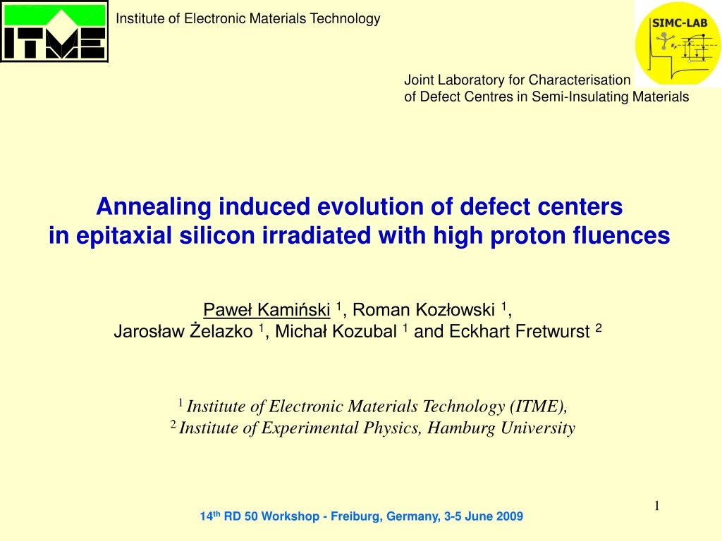
Institute of Electronic Materials Technology Joint Laboratory for Characterisation of Defect Centres in Semi-Insulating Materials Annealing induced evolution of defect centers in epitaxial silicon irradiated with high proton fluences Paweł Kamiński1, Roman Kozłowski1,Jarosław Żelazko1, Michał Kozubal 1 and Eckhart Fretwurst 2 • 1 Institute of Electronic Materials Technology(ITME), 2 Institute of Experimental Physics, Hamburg University 14th RD 50 Workshop -Freiburg, Germany,3-5June 2009
Outline • Samples – pad detectors based on epitaxial silicon irradiated with high proton fluence • Details of HRPITS measurements • HRPITS images of spectral fringes for radiation defects in standard (ST) and oxygenated (DO) epitaxial layers before and after 1-h isochronal annealing • Comparison of defect levels in ST and DO epitaxial silicon • Comparison of defects concentrationsin ST and DO epitaxial silicon • Conclusions
Samples • Epitaxial n-Si pad-detectors on Cz-substrate produced by ITME/CiS • Resistivity : 500 Wcm,Thickness: ~ 150 μm, Size: 5 x 5 mm2 • Standard (ST) and oxygen enriched (DO, diffusion for 24h at 1100°C) material • 24 GeV/c-proton-irradiation (CERN PS), eq = 1.71 x 1016 cm-2 From: Charge collection and trapping effects in 75 μm, 100 μm and 150 μm thick n-type epitaxial silicon diodes after proton irradiation Julian Becker, Eckhart Fretwurst, Jörn Lange, Gunnar Lindström, Hamburg University ,13th RD50 Workshop, CERN, November 2008
Imaging of defect levels for as-irradiated samples and after following annealing stages: HT1: 1h, 80 oC + 24 h, RT HT2: (1h, 80 oC + 24 h, RT) + 1h, 160 oC + 24 h, RT HT3: (1h, 80 oC + 24 h, RT + 1h, 160 oC + 24 h, RT) + 1h, 240 oC + 24 h, RT
Details of HRPITS measurements • Temperature range: 30 – 300 K, DT = 2 K • Excitation source: 1 mW, 650 nm laser diode (hn = 1.908 eV) • Excitation pulse parameters: Period – 250 ms, Width – 50 ms • Photon flux: 1.3x1017 cm-2s-1 • BIAS: 20 V • Gain: 1x10⁶ – 1x10⁸V/A • AVG: 250 waveforms • Analysis of photocurrent relaxation waveforms: • - 2D correlation procedure (multi-window approach) images of correlation spectral fringes for radiation defect centres • - 2D inverse Laplace transformation algorithm images of Laplace fringes for radiation defect centres
Effect of annealing on mobility lifetime product fluence 1.7x10¹⁶ p/cm2 standard epilayer oxygenated epilayer
HRPITS images – fluence 1.7x10¹⁶ p/cm2 – as-irradiated standard epilayer oxygenated epilayer
HRPITS images – fluence 1.7x10¹⁶ p/cm2 – 80 oC standard epilayer oxygenated epilayer
HRPITS images – fluence 1.7x10¹⁶ p/cm2 – 160 oC standard epilayer oxygenated epilayer
HRPITS images – fluence 1.7x10¹⁶ p/cm2 – 240 oC standard epilayer oxygenated epilayer
Comparison of defect levels in standard and oxygenated epitaxial silicon; 1.7x10¹⁶ p/cm2; as-irradiated eTm = AmT2exp(-Eam / kBT);Amn = gnsmn; Amp = gpsmp TS8, TS7, TC1 : shallow donors-STD(H); TS9, TS10, TC2: I aggregates; T7: V2(+/0); TA4: VO(-/0); TA6: V2(-/0); TA7: V4V5;TA8: complex of O with V aggregates (V4,V5);TS5: IO2 (?) standard, m = 1,2…13 oxygenated, m = 1,2…10
Comparison of defect levels in standard and oxygenated epitaxial silicon; 1.7x10¹⁶ p/cm2; annealing at 80 oC TA1: shallow donors; TA2: I aggregates; TA4: VO(-/0); TS5: IO2 (?) TA6: V2(-/0); T7: V2(+/0); TA7: V4V5;TA8: complex of O with V aggregates (V4,V5); standard, m=1,2…13 oxygenated, m =1,2…11
Comparison of defect levels in standard and oxygenated epitaxial silicon;1.7x10¹⁶ p/cm2; annealing at 160 oC TA1: shallow donors; TA2, TS3: I aggregates; TA4: VO(-/0); TA6:V2(-/0); T7: V2(+/0); TA7: V4V5; TA8: complex of O with V aggregates (V4,V5) standard, m=1,2…12 oxygenated, m=1,2…10
Comparison of defect levels in standard and oxygenated epitaxial silicon; 1.7x10¹⁶ p/cm2; annealing at 240 oC TA1: shallow donor; TS1,TA2, TS2, T1, T2, T3, T4: I aggregates; T7: V2(+/0); TA4: VO(-/0); TA6: V2(-/0);T8: V2O (2-/-);T13: I center (V3); T14: V aggregate (V5) standard, m=1,2…13 oxygenated, m=1,2…14
Comparison of defects concentrations in standard and oxygenated epitaxial silicon; 1.7x10¹⁶ p/cm2 ; as-irradiated TS7, TS8, TC1 : shallow donors; TS9, TS10, TC2: I aggregates; T7: V2(+/0); TA4: VO(-/0); TA6: V2(-/0); TA7: V4V5; TA8: complex of O with V aggregates (V4,V5);TS5: IO2 (?) standard oxygenated
Comparison of defectsconcentrations in standard and oxygenated epitaxial silicon; 1.7x10¹⁶ p/cm2; annealing at 80 oC TA1: shallow donors; TA2: I aggregates; TA4: VO(-/0); TS5: IO2 (?) TA6: V2(-/0); TA7: V4V5; T7: V2(+/0); TA8: complex of O with V aggregates (V4,V5); standard oxygenated
Comparison of defectsconcentrations in standard and oxygenated epitaxial silicon; 1.7x10¹⁶ p/cm2 ; annealing at 160 oC TA1: shallow donors; TA2, TS3: I aggregates; TA4: VO(-/0); TA6:V2(-/0); T7: V2(+/0);TA7: V4V5; TA8: complex of O with V aggregates (V4, V5) standard oxygenated
Comparison of defects concentrations in standard and oxygenated epitaxial silicon; 1.7x10¹⁶ p/cm2; annealing at 240 oC TA1: shallow donor; TS1,TA2, TS2, T1, T2, T3, T4: I aggregates; T7: V2(+/0); TA4: VO(-/0); TA6: V2(-/0);T8: V2O (2-/-);T13: I center (V3); T14: V aggregate (V5) standard oxygenated
Conclusions • For the first time we have shown the results of both qualitative and quantitative analysis of defect levels for epitaxial silicon after 24 GeV/c protons irradiation with a fluence of 1.7x1016 cm-3. The radiation defect levels have been scanned by High-Resolution Photoinduced Transient Spectroscopy with implementation of the imaging procedure. • The effect of the oxygen concentration in the epitaxial layers on the traps properties and concentrations was studied. It was found that the higher oxygen concentration affects mainly the properties of shallow traps related to interstitial aggregates. After annealing at 240 oC, the high concentrations of midgap traps with activation energies of 565 and 575 meV are observed independently on the oxygen concentration. • After annealing at 80 and 160 oC, the greatest number of the same traps was observed both for standard and oxygenated epitaxial layers. • Further studies aimed at verifying the values of traps concentrations are in progress.
Acknowledgments We thank Prof.Gunnar Lindstroem for initiating the WODEAN collaborationand stimulating discussions. This work was carried out within the framework of the RD 50 project with financial support of the Polish Ministry of Science and Higher Education under grant No. CERN/15/2007.
im(t, T) = Im(l, T)exp(-eTmt); Im (l, T) = ntom(T ) eTm(T ) T (T ) T (T ) C (,T )qE M i(t, T) = Ik (l, T)exp(-eTmt); m=1 eTm = AmT2exp(-Eam / kBT) Amn = gnsmn; Amp = gpsmp Model of Photocurrent Relaxation Waveforms For Si: gn= 1.07 x 1021cm-2K-2s-1;gp= 2.64 x 1021cm-2K-2s-1