Download
1 / 13
150 likes | 345 Views
Direct Observation of a Widely Tunable Bandgap in Bilayer Graphene Yuanbo Zhang et al , Nature (2009). Wonjun Park School of Electrical and Computer Engineering Purdue University. Outline. • Introduction Device structure Structure of bilayer graphene

E N D
Direct Observation of a Widely Tunable Bandgap in BilayerGraphene Yuanbo Zhang et al, Nature (2009) • Wonjun Park • School of Electrical and Computer Engineering • Purdue University
Outline • •Introduction • Device structure • Structure of bilayergraphene • Displacement field & bandgap • Electrical resistance & CNP • Absorption spectra • Summary
Introduction • • Gapless feature in graphene Sloppy on/off ratio • • Bandgapengineering : GNR, Nanomesh • Tunable bandgap : Great flexibility in design and • optimization in devices • Dual-gate bilayergraphene Up to ~250 meV,
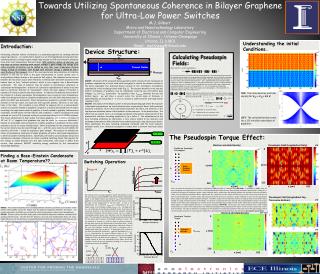
Device Structure • S/D : Au (30 nm) • Top gate : Pt (20 nm) • Bottom gate : Si • Top gate insulator : Al2O3 (dt=80 nm, εt=7.5 ) • Bottom gate insulator : SiO2 (db=285 nm, εb=3.9 )
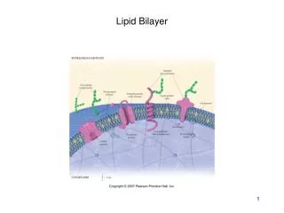
Structure of Bilayergraphene A-B stacked Bilayer1 • Without gating, the lowest CB and • highest VB touch each other at K. • With E-field, the bandgap occurs due • to symmetry breaking with respect to • charge and electrostatic potential. 1. Tsung-Ta Tang et al. Nature (2009)
Displacement Field D & Bandgap • Electrical displacement field D • Db=εb (Vb-Vbo)/db & Dt=- εt (Vt-Vto)/dt where • Vo is effective offset due to environmental • doping • δD=Db-Dt Net carrier doping(n) EF shift • δD = 0 Charge neutral point (CNP) • Ď=(Db+Dt)/2 Breaking inversion symmetry • Non-zero bandgap • By setting δD=0 and changing Ď Bandgap • changes while keeping grphene in CNP • By changing δD and maintaining Ď EF • shifts but bandgap is maintained. • Δ~84Ď+34.7sin(Ď) for Ď < 3V/nm1
Electrical Resistance & CNP CNP • Resistance varies due to induced-bandgapΔ • Each peak is CNP • Low peak originates from small Δ • We can find CNP at zero gap. (Dt= Db =0) in the lowest • resistance Vto~-5V, Vbo~10V • δD=Db-Dt=0 Vt=-(εb dt/ εt db)Vb+contant, |Slope|~0.15
Absorption Spectra at Strong Field γ=400meV • Background : zero bandgap CNP (Ď=0) • Peak at 300 meV : Transition I due to bandgap opening • Dip at and above 400 meV : Transition II~V • As Δ increases, the peaks related to Transition I shift to higher • and become stronger due to increase in DOS at band edge • Bandgap tuning up to 250 meV • Fano interference : G-mode phonon (1585cm-1~200 meV) + • Continuous electronic transition
Absorption Spectra at Weak field • Difficult to measure bandgap directly at low field • Difference between CNP(δD=0) and δD=0.15Vnm-1 • Transition IV is stronger & suppressed transition III • Red shift of IV lower conduction band move up • Shift~Δ/2
Summary • Bandgap can be induced in bilayergraphene by gating bias, which breaks the symmetry between top and bottom layer. • Bandgap opening was demonstrated via IR Strong field Bandgap opening Blue shift (Tran. I) • Bandgap transition is strong (~5% absorption) enough as strong oscillator Novel nanophotonic devices such as IR generation, amplification, and detection.
Q&A Thank you…Any Question?
Note A(E)-Ae Center energy EΩ, line width γ q : relative dipole strength of phonon and electron transition Ve-p:electron-phonon coupling De-h :joint electron-hole pair density μ : dipole moment