Download
1 / 15
160 likes | 307 Views
This document outlines the critical specifications for RF amplifier analysis and design, including input and load impedance, operating frequencies, maximum power output, voltage and power gains, and efficiency metrics. It emphasizes that design is the reverse of analysis, highlighting the differences between analysis problems (which have a single solution) and design problems (which may have multiple solutions). The material covers various equivalent circuits, bias analysis, and AC models essential for effective amplifier design, alongside practical examples and performance summaries.

E N D
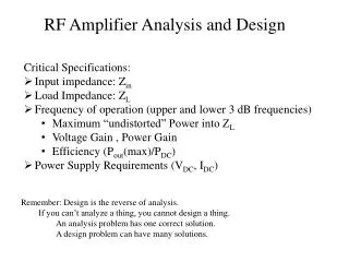
RF Amplifier Analysis and Design • Critical Specifications: • Input impedance: Zin • Load Impedance: ZL • Frequency of operation (upper and lower 3 dB frequencies) • Maximum “undistorted” Power into ZL • Voltage Gain , Power Gain • Efficiency (Pout(max)/PDC) • Power Supply Requirements (VDC, IDC) Remember: Design is the reverse of analysis. If you can’t analyze a thing, you cannot design a thing. An analysis problem has one correct solution. A design problem can have many solutions.
Transistor Equivalent Circuits Equivalent AC Model For Amplifier Analysis/Design (Common Emitter) AC Model For Amplifier Analysis/Design (Common Base) DC Model For Bias Analysis/Design
Typical RF Amplifier DC Equivalent AC Equivalent
Book Example: Fig 1-11 DC/Bias Analysis Assume b is large, so IB can be neglected. Then: Compute IE Compute re Check Assumption 1. Current through the base bias resistors is 1 mA. The base current can be neglected if it is less than 5% of the resistor current, or .05 mA. …Since b > 25, our assumption is valid 12 v 10 kW VB 2 kW 1 kW
Parasitic Coil Resistance AC Analysis Transformed Load Resistance Total AC Collector Resistance Transistor Voltage Gain Include the transformer: This is a general result that we will use over and over again! (eq 1-24)
Frequency Analysis Input Impedance (b = 50) Power Gain
vC VCC IC Saturation Margin VE Cutoff Margin
AC Load Line iC Saturation: vCE ~ 0 For Symmetrical Clipping: If Then cutoff limits amplitude. If Then saturation limits amplitude. Q Point (quiescent) IC Cutoff: iC~ 0 vCE VCE Max P-P Undistorted Collector Voltage Swing
Example 1-4 AC Load Line(Fig 1-11) iC 5.1 mA Maximum Undistorted Power Output IC = 1.3mA 14.2 v vCE VCE = 10.7 v This will occur when the input voltage is 26 mv 0-pk or 18 mv RMS Max P-P Undistorted Collector Voltage Swing: V0-pk = 3.5 v
Discussion Since the author neglected to do the load line analysis, he failed to detect the fact that with 40 mV rms input (56.5 mV 0-pk), the collector voltage would want to swing 7.7 V 0-pk. Since the maximum 0-pk voltage swing determined by the load line is 3.5 V the amplifier will go into cutoff and the tops of the sine waves will be clipped. Design is all about verification/validation and iteration. For this DC bias scheme, the optimum total AC collector resistance at resonance should be : …which is greater than the transformed load resistance of 7.2 kW. If the 5 kW resistor were eliminated, we would have This is still less than Rc’(opt), but . . ..
. . . We can make Rc’ = Rc’(opt) if we can make This requires a transformer turns ratio of: Now and . . . and the gains are:
New AC Load Line iC 2.56 mA Maximum Undistorted Power Output IC = 1.3mA 21.7 v vCE VCE = 10.7 v Limited by saturation Max P-P Undistorted Collector Voltage Swing: V0-pk = 10.7 v This will occur when the input voltage is 25.2 mv 0-pk or 17.3 mv RMS
Performance Summary The table below summarizes the performance changes introduced by removing the 5k resistor and changing the turns ratio from 12 to 15:
Voltage, Current, and Power Assume Maximum Power Output Condition: Ic = IC Vce = VCE For the AC Collector Load: For the Transistor: